Integrated optical sensor package
An integrated light and ambient light sensor technology, which is applied in the direction of electric solid-state devices, semiconductor devices, semiconductor/solid-state device components, etc., can solve the problems of high manufacturing cost and large sensor packaging volume, so as to reduce production cost and simplify the process Preparation, volume reduction effect
- Summary
- Abstract
- Description
- Claims
- Application Information
AI Technical Summary
Problems solved by technology
Method used
Image
Examples
Embodiment Construction
[0032] The technical solutions adopted by the present invention in order to achieve the purpose are further described below in conjunction with the accompanying drawings and the embodiments of the present invention.
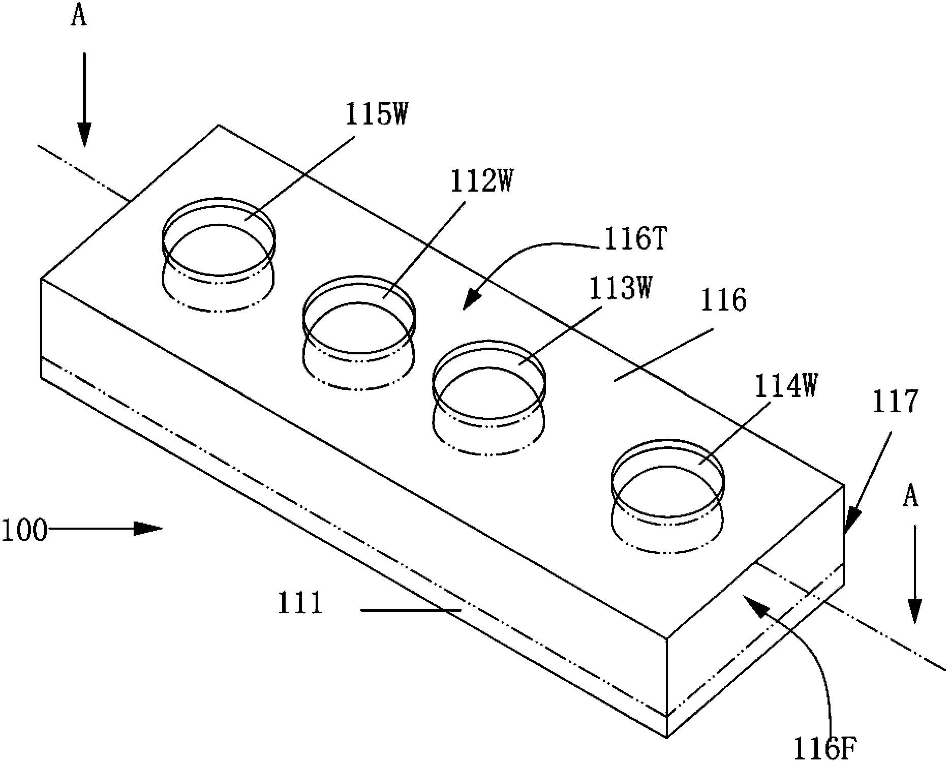
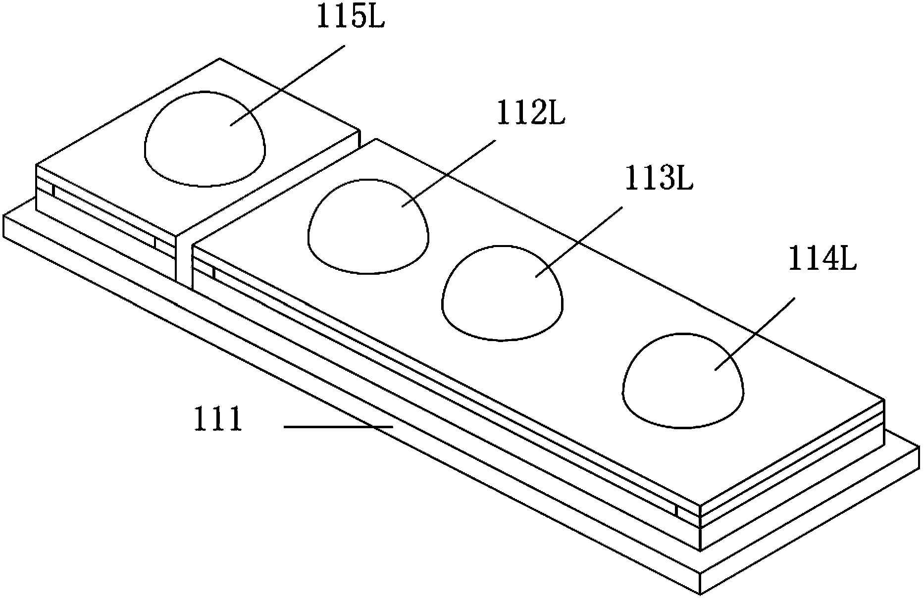
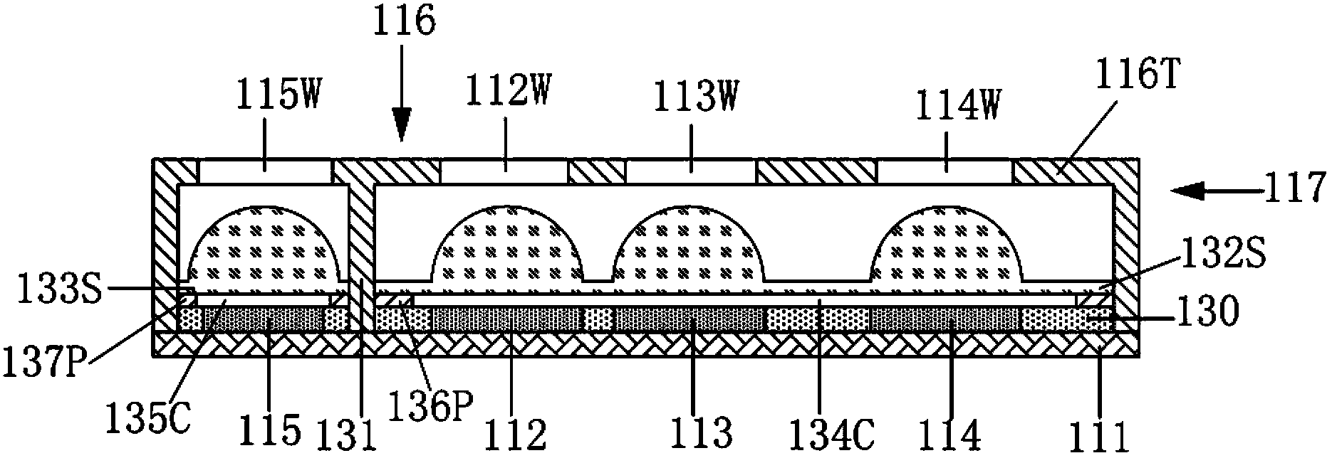
[0033] The present invention provides an integrated photosensor package, comprising:
[0034] The package substrate at the bottom;
[0035] An ambient light sensor, a proximity light sensor, and an image sensor located on the packaging substrate;
[0036] The package cover is sealed with the package substrate to form a package case.
[0037] In an embodiment of the present invention, the integrated photosensor package further includes an infrared light emitter located in the package housing. In addition, the infrared light transmitter includes an infrared LED and a driving circuit.
[0038] Further, there are lenses above the infrared light emitter, the ambient light sensor, the proximity light sensor and the image sensor respectively. In the manufacturing pr...
PUM
 Abstract
Description
Claims
Application Information
 - R&D
- Intellectual Property
- Life Sciences
- Materials
- Tech Scout
- Unparalleled Data Quality
- Higher Quality Content
- 60% Fewer Hallucinations
Browse by: Latest US Patents, China's latest patents, Technical Efficacy Thesaurus, Application Domain, Technology Topic, Popular Technical Reports.
© 2025 PatSnap. All rights reserved.Legal|Privacy policy|Modern Slavery Act Transparency Statement|Sitemap|About US| Contact US: help@patsnap.com


