Method for producing double embedded structure

A dual damascene structure and manufacturing method technology, which is applied in semiconductor/solid-state device manufacturing, electrical components, circuits, etc., can solve problems such as heavy impact and thermal stress, simplify the process, reduce the impact of thermal stress, and save production costs Effect

Active Publication Date: 2008-10-01
UNITED MICROELECTRONICS CORP
View PDF5 Cites 0 Cited by
  • Summary
  • Abstract
  • Description
  • Claims
  • Application Information

AI Technical Summary

Problems solved by technology

However, for low dielectric materials, thermal stress (thermal strcss) can have a serious impact, especially for organic spin-on materials like SiLK (aromatic hydrocarbons), etc.

Method used


Image

  • Method for producing double embedded structure
  • Method for producing double embedded structure
  • Method for producing double embedded structure

Examples


Embodiment Construction

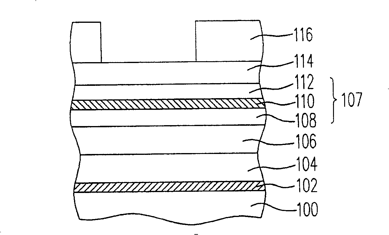
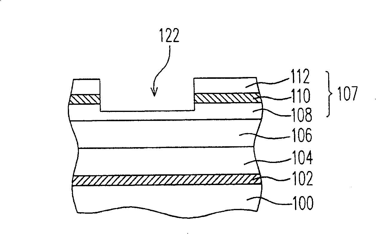
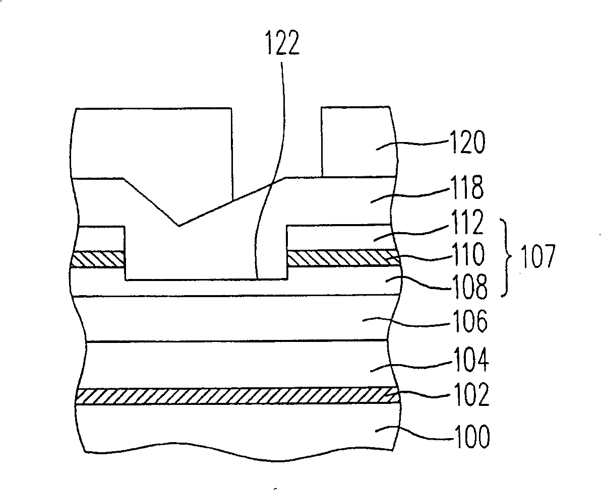
[0051] Figure 1A to Figure 1I It is a cross-sectional view showing the process of a method for manufacturing a dual damascene structure according to a preferred embodiment of the present invention. First, please refer to Figure 1A, forming a barrier layer 102 on the substrate 100 . Wherein, the material of the barrier layer 102 is, for example, one of silicon nitride, silicon carbide, and silicon carbonitride. Next, a first dielectric layer 104, a second dielectric layer 106, a multilayer mask layer 107, a first bottom anti-reflection layer 114, and a first photoresist layer (not shown) are sequentially formed on the barrier layer 102 drawn). Wherein, the multi-layer mask layer 107 is composed of, for example, a cover layer 108 , a metal-containing hard mask layer 110 , and a dielectric hard mask layer 112 . In another embodiment, the multi-layer mask layer may also be composed of a cover layer and a metal-containing hard mask layer. In addition, the material of the firs...


PUM


Abstract

This invention relates to a method for manufacturing double mosaic structure, which first of all forms a block layer, a first dielectric layer, a second dielectric layer, a multi-layer mask layer, a first bottom anti-reflection layer and a pattern first photo resist layer orderly on a substrate, then takes the pattern first photo resist layer as the mask to etch to get a first channel structure, then forms a second bottom anti-reflection layer to fill the first channel structure and cover the surface of the multi-layer mask layer, after that, forms a second photo resist layer on the second bottom anti-reflection layer to be taken as the mask to etch it to get a first medium window structure, then etches the first channel structure and the first medium window structure to get a second channel structure and a second medium structure.

Description

technical field [0001] The invention relates to a method for manufacturing a semiconductor element, in particular to a method for manufacturing a double damascene structure. Background technique [0002] In current semiconductor processes, copper metal is mostly used to make metal interconnections because copper metal itself has the advantages of low resistivity and the ability to avoid electromigration. In addition, because the etching of copper metal is not easy, a damascene process is used to replace the traditional process to produce copper wires. [0003] As the width of semiconductor devices continues to shrink, the signal transmission delay (resistance capacitance time delay) caused by multiple metal interconnections becomes a very important factor. Therefore, in the current technology, a low dielectric constant material layer is used to cooperate with copper metal wires to improve the performance of the device. Moreover, if a porous low dielectric constant film wit...

Claims


Application Information

Patent Timeline
Patent Type & Authority Patents(China)
IPC IPC(8): H01L21/768
Inventor 王志荣
Owner UNITED MICROELECTRONICS CORP
Why Eureka
Try Eureka