Power module by directly bonding power terminal

A power terminal, direct bonding technology, applied in the field of power electronics, can solve the problem of large parasitic inductance, reduce the influence of thermal stress, and improve the performance.

Active Publication Date: 2012-05-30
斯达半导体股份有限公司
View PDF3 Cites 0 Cited by
  • Summary
  • Abstract
  • Description
  • Claims
  • Application Information

AI Technical Summary

Problems solved by technology

[0004] The present invention aims to solve the problem of large parasitic inductance caused by power terminals inside the existing power module

Method used


Image

  • Power module by directly bonding power terminal
  • Power module by directly bonding power terminal
  • Power module by directly bonding power terminal

Examples


Embodiment Construction

[0009] The present invention will be further described below in conjunction with the accompanying drawings and embodiments.

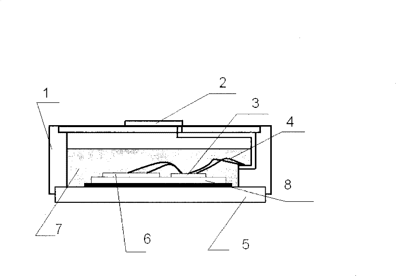
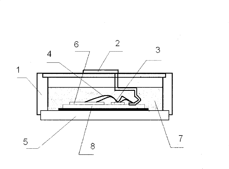
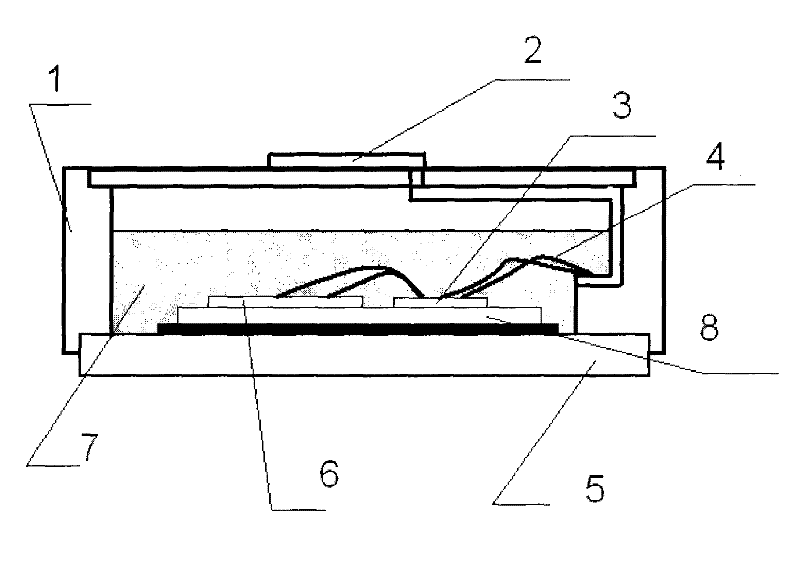
[0010] The power module in this embodiment is an insulated gate bipolar transistor (IGBT) module. Such as figure 1 As shown, the present invention includes an insulated gate bipolar transistor chip 7, a diode chip 3, an insulating substrate (DBC) 5, a heat sink 6, a power terminal 2, an aluminum wire 4, a plastic shell 1 and a silicone gel 8, and an insulated gate bipolar transistor The polar transistor chip 7 and the diode chip 3 are reflow welded on the conductive copper layer of the insulating substrate (DBC) 5, and the insulating substrate (DBC) is directly welded on the heat dissipation plate 6 by brazing. The power terminal 2 is directly fixed on the housing 1 . Between each chip (insulated gate bipolar transistor chip 7, diode chip 3), between each chip (insulated gate bipolar transistor chip 7, diode chip 3) and the corresponding conductive l...


PUM


Abstract

The invention discloses a power module by directly bonding a power terminal, comprising a chip, an insulating substrate, a radiating rib, the power terminal and a shell, wherein the power terminal is directly fixed on the shell. The fixing mode of the power terminal can optimize the design shape of the terminal, reduce stray inductance, and improve the reliability and service life by applying thepower terminal module.

Description

technical field [0001] The invention belongs to the field of power electronics and relates to packaging of power modules, in particular to a power module with direct bonding of power terminals. Background technique [0002] Power modules include insulated gate bipolar transistor (IGBT) modules, diode modules, MOSFET modules, intelligent power (IPM) modules, etc. There are some inherent shortcomings in the traditional packaging of these power modules. figure 2 Be explained. figure 2 Shown is a conventional IGBT module package. A traditional IGBT module includes an IGBT chip 7, a diode chip 3, an insulating substrate (DBC) 5, a heat sink 6, power terminals 2, aluminum wires 4, a plastic case 1, and silicone gel 8 . Depend on figure 2 It can be seen that the traditional power terminal 2 is soldered to the conductive copper layer on the surface of the insulating substrate (DBC) 5 by reflow soldering. Because the coefficient of thermal expansion of the solder used is quite ...

Claims


Application Information

Patent Timeline
Patent Type & Authority Patents(China)
IPC IPC(8): H01L25/00H01L23/48H01L23/488H01L23/02
CPCH01L2924/13091H01L2224/48091H01L2224/45124H01L24/13H01L2924/30107H01L2924/13055H01L2224/13H01L2924/1305H01L2924/351H01L2924/00014H01L2924/00H01L2924/00012
Inventor 姚礼军刘志宏金晓行胡少华张宏波雷鸣余传武沈华
Owner 斯达半导体股份有限公司
Why Eureka
Try Eureka