
MTJ stack and bottom electrode patterning process with ion beam etching using a single mask

a technology of etching process and mask, which is applied in the manufacture/treatment of electrical equipment, magnetic device, and semiconductor devices. it can solve the problems of not being able to control the size of mtj and its uniformity for scalability, and not being able to find a hard mask material with enough selectivity for use with rie, etc., to achieve the effect of improving selectivity

Active Publication Date: 2015-10-20
AVALANCHE TECH
View PDF21 Cites 39 Cited by
  • Summary
  • Abstract
  • Description
  • Claims
  • Application Information

AI Technical Summary

Benefits of technology

[0016]In an alternative embodiment the MTJ etch starts with RIE, and RIE stops prior to the barrier layer. The remaining MTJ stack and the bottom electrode are etched by IBE. This prevents MTJ damage by the RIE chemistry.
[0018]Second set of embodiments: MTJ sidewall is protected by depositing dielectric material after MTJ etching and prior to IBE bottom electrode etching. This prevents the barrier layer from incurring plasma damage. In some embodiments, an oxygen free dielectric material is preferred.

Problems solved by technology

It is, however, difficult to find a hard mask material with enough selectivity for use with RIE.
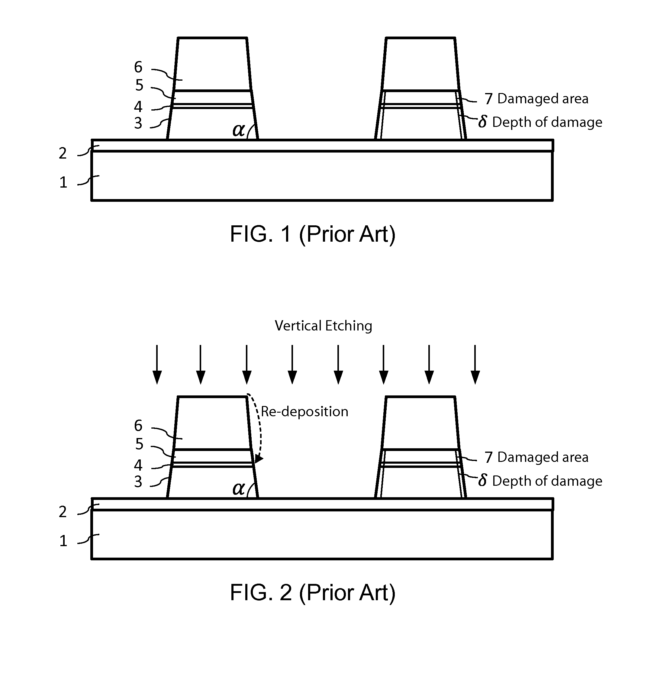
Re-deposition of etched material on the sidewall is also a serious concern, because it can make it the device inoperable by forming an electrical short across the barrier layer.
However, it is not desirable for controlling the MTJ size and its uniformity for scalability.
This amount of top electrode thickness loss is not desirable and would make downstream interconnect process difficult.
It is not desirable to expose MTJ sidewall to atmosphere for wet cleaning.
Specifically, IBE etching selectivity of a hard mask layer versus magnetic materials is not as desirable as that of a chemical etch process such as RIE.
On the other hand, MTJ components are sensitive to being degraded by the chemical etching ambient, which often degrades TMR (tunnel magneto-resistance).
It has been found that the etched surface of MTJ, including the sidewall edge, is damaged in plasma ambient.
Another issue is the process sequence and complexity.
However, separate patterning is not mandatory for STT (Spin Transfer Torque) MRAM.
While it is less challenging to fabricate the device from etch point of view, there is a trade-off with process complexity, manufacturing cost, as well as extendibility to high density.
In addition to the photo-mask required to pattern MTJ stack, an extra mask is needed to define bottom electrode, which complicates the process flow due to required planarization after each photo processing step, overlay margin tolerance, etc.
Also a small cell area cannot be achieved with BE size larger than MTJ size, so this limits extendibility.

Method used


Image

  • MTJ stack and bottom electrode patterning process with ion beam etching using a single mask
  • MTJ stack and bottom electrode patterning process with ion beam etching using a single mask
  • MTJ stack and bottom electrode patterning process with ion beam etching using a single mask

Examples


first embodiment

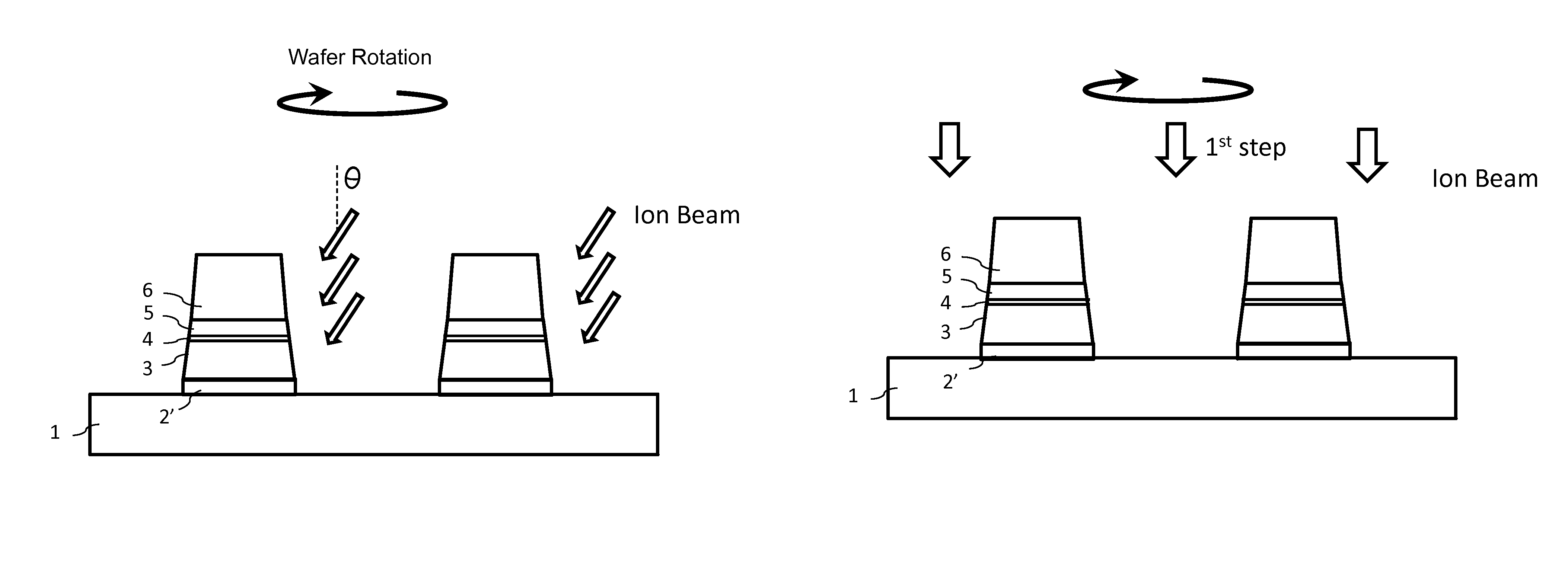
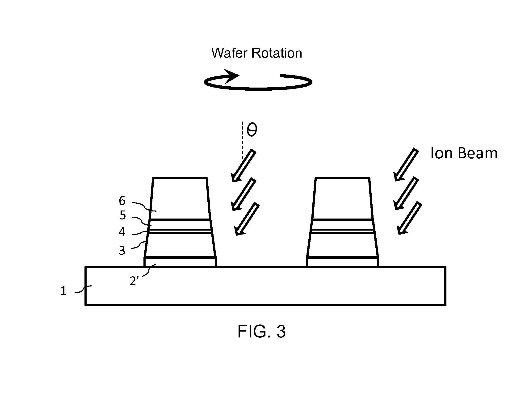
[0035]An alternative of the first embodiment separates the IBE bottom electrode etching into 2 steps as shown in FIGS. 4A & 4B. In FIG. 4A the 1st step is designed to remove the exposed bottom electrode material with a first angle which is preferably a low angle of incidence (e.g. close to normal) selected to efficiently remove the unneeded bottom electrode material. In some cases, a higher etching angle is effective to remove the bottom electrode but is susceptible to re-deposition. As shown in FIG. 4B, the 2nd step is to clean the sidewall with a second incident angle, higher than the first angle.

[0036]Variations of the first embodiment include etching the MTJ stack with processes with reduced chemical damage including ICP using inert gas such as Ar or Kr, or a mixture of Ar or Kr with other gases such as CH3OH, CO, NH3, etc. This step is followed by the bottom electrode etching with angle IBE for sidewall re-deposition cleaning.

[0037]Etch rate of RIE including MICP using inert ga...

third embodiment

[0040]the invention includes self-adjustment of MTJ CD (Critical Dimension) with angled IBE. Etch rate of IBE depends on the specific materials as well as the incident angle as shown in FIG. 7. In this example the etch rate is highest at an incident angle of 50 degrees. The etch rate can be separated into vertical and horizontal components which vary with the incident angle of IBE. By varying the incident angle (a1, a2, a3), the bottom slope of MTJ can be changed as shown in FIG. 8 due to different etch rates. The higher angles, such a3, result in greater etching of the lower magnetic layer 3. The lowest angles, such a1 in this example, result in relatively less etching of the lower magnetic layer 3. By selecting an optimal angle, the slope of the bottom of the MTJ can be formed as steep as desired. Control of the slope of the bottom of the MTJ is advantageous for control the CD. A steep side wall makes it easier to control the CD.

[0041]FIG. 8 illustrates that the choice of IBE angl...


PUM


Abstract

Fabrication methods using Ion Beam Etching (IBE) for MRAM cell memory elements are described. In embodiments of the invention the top electrode and MTJ main body are etched with one mask using reactive etching such as RIE or magnetized inductively coupled plasma (MICP) for improved selectivity, then the bottom electrode is etched using IBE as specified in various alternative embodiments which include selection of incident angles, wafer rotational rate profiles and optional passivation layer deposited prior to the IBE. The IBE according to the invention etches the bottom electrode without the need for an additional mask by using the layer stack created by the first etching phase as the mask. This makes the bottom electrode self-aligned to MTJ. The IBE also achieves MTJ sidewall cleaning without the need for an additional step.

Description

RELATED APPLICATION[0001]The present application is related to U.S. provisional patent application Ser. No. 61 / 734,519, filed Dec. 7, 2012, by SATOH et al., which is included by reference herein and for which benefit of the priority date is hereby claimed.FIELD OF THE INVENTION[0002]The present invention relates to the techniques for fabricating arrays of magnetoresistive random access memory (MRAM) cells such as those including magnetic tunnel junctions (MTJ) memory elements on wafers. The invention relates more particularly to etching processes for fabricating magnetic tunnel junction (MTJ) stacks and the bottom electrode.BACKGROUND OF THE INVENTION[0003]FIG. 1 illustrates a cross sectional view of a selected stage in the prior art fabrication process of MTJ MRAM arrays after MTJ etching. A memory element of MRAM typically includes of a bottom electrode, a MTJ (Magnetic Tunnel Junction) and a top electrode (TE) 6. The top electrode layer 6 can be a single layer metal or multi-laye...

Claims


Application Information

Patent Timeline
Patent Type & Authority Patents(United States)
IPC IPC(8): H01L29/04H01L43/12
CPCH01L43/12H10N50/01
Inventor SATOH, KIMIHIROJUNG, DONG HAZHANG, JINGCHEN, BENJAMINHUAI, YIMINGRANJAN, RAJIV YADAVZHOU, YUCHEN
Owner AVALANCHE TECH
Learn More