
Methods and systems for determining trapped charge density in films

a technology of trapped charge density and film, applied in the field of semiconductor/solid-state device testing/measurement, can solve the problems of poor transistor drive current due to degraded field effect carrier mobility, inability to determine the extent of charge trapping, and inability to achieve the effect of increasing the accuracy of determining

Inactive Publication Date: 2009-09-29
SEMATECH
View PDF3 Cites 16 Cited by
  • Summary
  • Abstract
  • Description
  • Claims
  • Application Information

AI Technical Summary

Benefits of technology

"The present patent provides a non-destructive and in-line technique for identifying charge trap densities in gate dielectric materials using a linear optical method. This technique uses spectroscopic data to determine the perturbation of the substrate dielectric function caused by the charge traps at the interface between a semiconductor material and a dielectric oxide layer. The method provides increased accuracy in determining the charge trap density compared to conventional modulation techniques. The technique can be used in the production of wafers and can provide valuable information on the quality of the interface between the semiconductor material and the dielectric oxide layer."

Problems solved by technology

As a result, leakage currents due to tunneling have increased, thereby inhibiting the performance of devices.
However, poor transistor drive current due to degraded field effect carrier mobility is a major issue with high-k dielectrics.
However, during the manufacturing process, there is no method available to determine the extent of charge trapping.
Unfortunately, current techniques to determine the extent of charge traps introduced into the dielectric film include electric capacitance-voltage (CV) measurements and current-voltage (IV) measurements, which are offline techniques.
This technique is an off-line, destructive technique (e.g., requiring sacrificial wafers for processing), and in many cases (especially high-k development), has failed to reflect the reality of the complex trapping structures in the dielectrics due to subsequent processing conditions such as high temperature anneal, gate electrode metal deposition, and the like.
However, modulation techniques are unable to accurately measure the charge trap induced changes in the substrate dielectric function because of the functional dependents of Seraphin coefficients (α and β) that act to scale the changes in the real or imaginary part of the dielectric function.
Thus, it would be difficult to extract information about the charge trap induced electric field without knowing exactly the thickness of the film, dielectric function of the film, and incident angle of each layer because modulations techniques do not provide thickness of films, dielectric function of film, and incident angles.
Any shortcoming mentioned above is not intended to be exhaustive, but rather is among many that tends to impair the effectiveness of previously known techniques for identifying charge traps in dielectric material; however, shortcomings mentioned here are sufficient to demonstrate that the methodologies appearing in the art have not been satisfactory and that a significant need exists for the techniques described and claimed in this disclosure.

Method used


Image

  • Methods and systems for determining trapped charge density in films
  • Methods and systems for determining trapped charge density in films
  • Methods and systems for determining trapped charge density in films

Examples


example 1

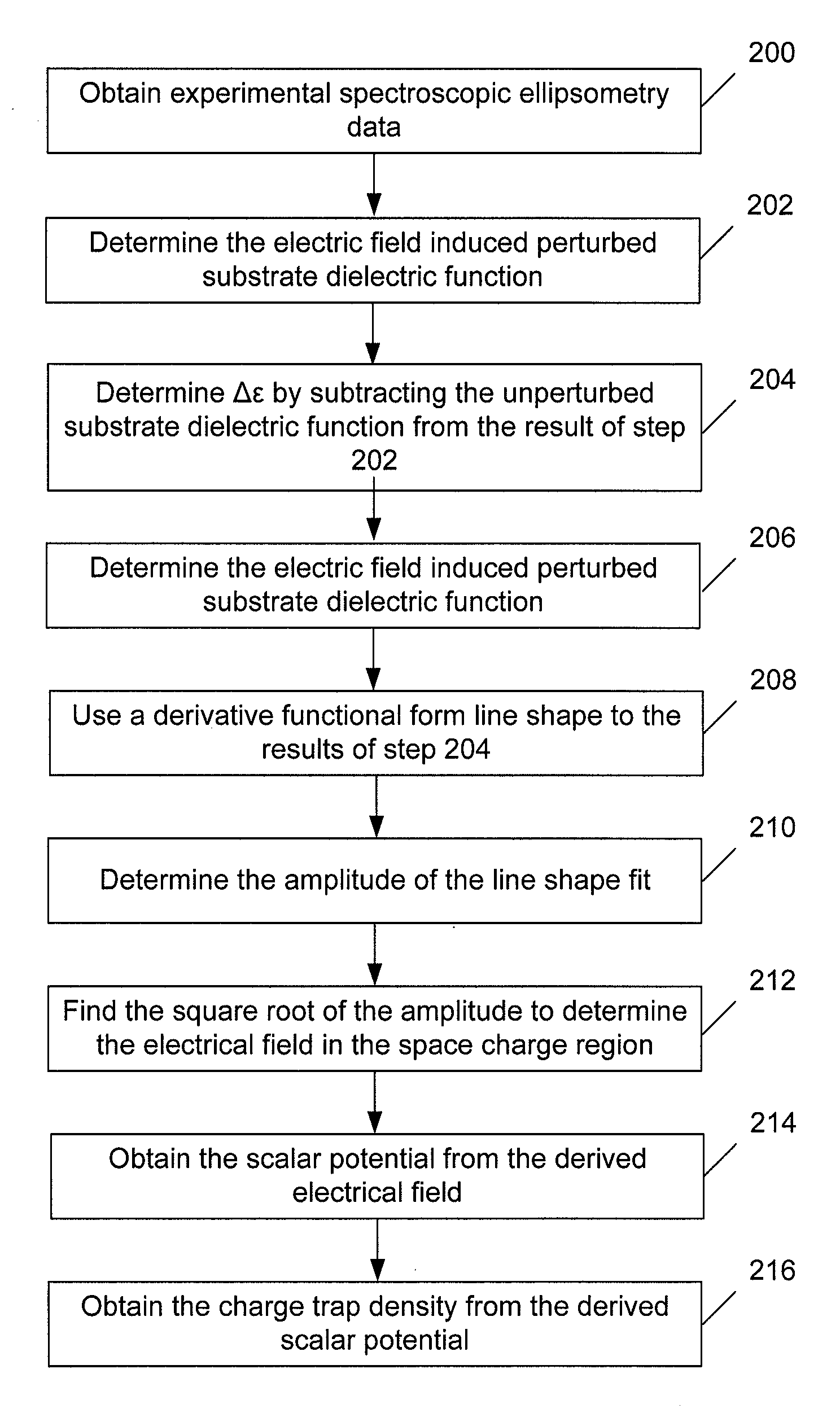
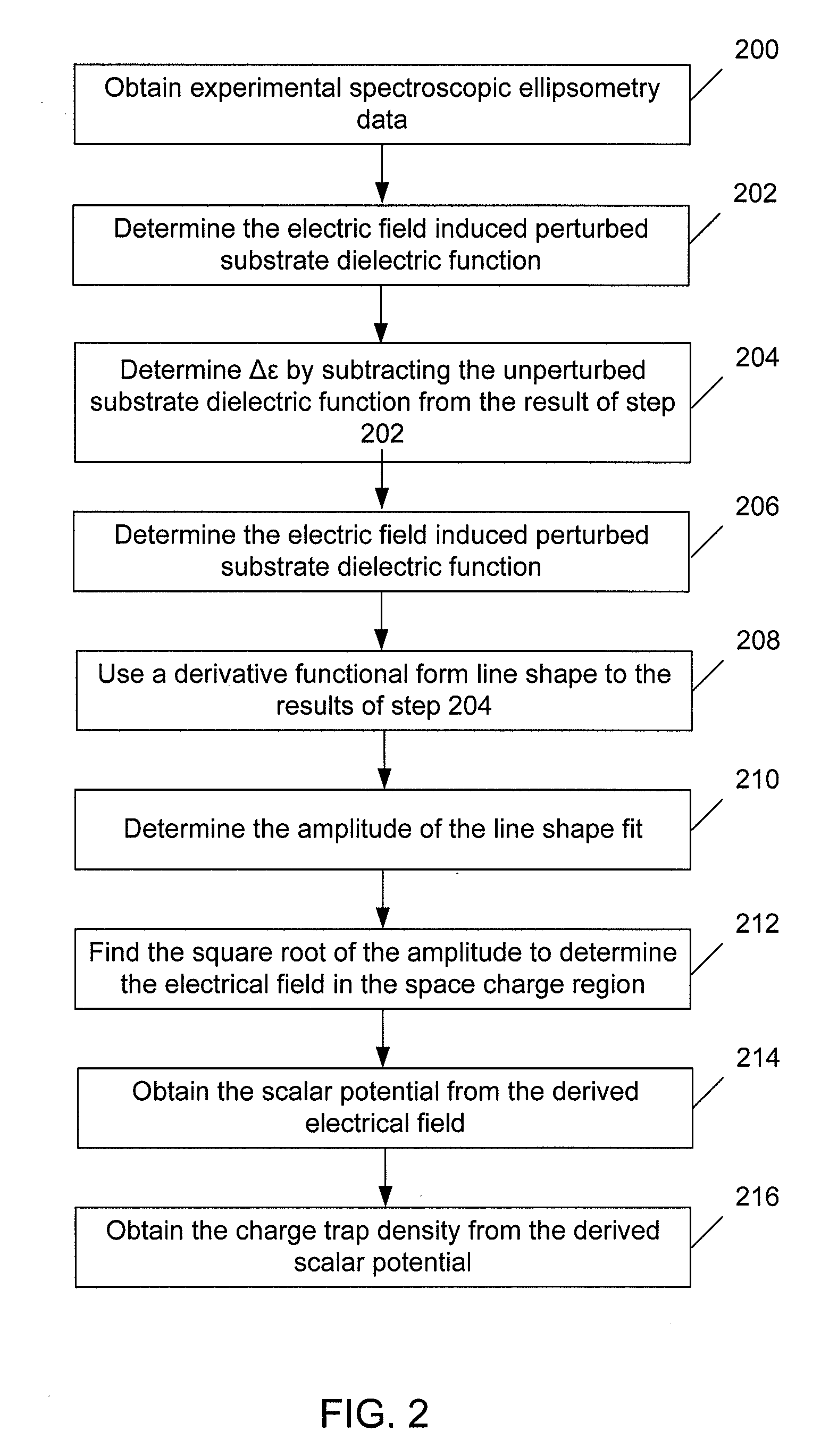
[0069]A first sample with substantially less charge trap density at the interface (e.g., HF cleaned silicon surface without a HfO2 film with a typical charge trap density of about 1×1010 cm−2 to 5×1010 cm−2) and a second sample with an expected high density of charge traps at the interface are tested using techniques of the present disclosure (e.g., using the steps described in FIG. 2). In particular, the first sample includes a (100)-oriented silicon surface (HF cleaned surface) having about 1.4 nanometers silicon dioxide (SiO2) layer. The second sample with the expected high density of charge traps includes a (100) silicon surface (HF cleaned surface) with an atomic layer deposited HfO2 layer having a thickness of about 3 nm and a typical charge trap density values of about 1×1011 cm−2 to 5×1011 cm−2.

[0070]Referring to FIG. 8, the amplitude of the silicon sample with the HfO2 layer (800) is about twice much as the silicon sample with silicon dioxide (802), as expected due to the a...

example 2

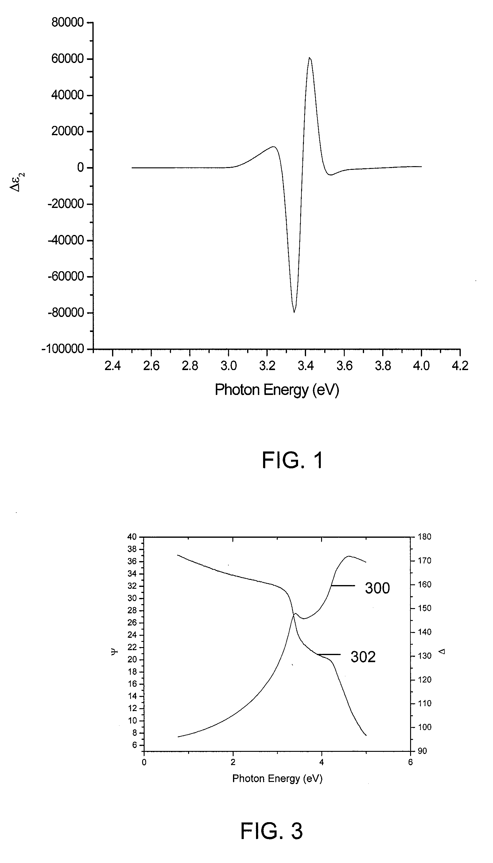
[0072]This example provides a correlation to second harmonic generation (SHG) results. First, five (100) silicon substrates were prepared with an initial HF last treatment followed by growth of the SiO2 interlayer using ozonated (O3) water (HCl 0.2%) using techniques known in the art. Following the surface clean, a 45% silicate (HfSiO) gate dielectric was deposited via atomic layer deposition (ALD) on each wafer. One wafer (wafer 900 of FIG. 9) was left as-deposited and received no further post deposition anneals, while the remaining four wafers were annealed in an NH3 ambient at 600° C. (wafer 902), 700° C. (wafer 904), 800° C. (wafer 906), and 900° C. (wafer 908). Spectroscopic ellipsometry data was taken on a J.A. Woollam Co. ellipsometer over the spectroscopic range of 0.75 eV −5.0 eV by 0.02 eV increments and an angle of incidence of 70-78 degrees by 4 degree increments.

[0073]The method of the present disclosure, for example, the method outlined in FIG. 2 was performed on each ...

example 3

[0075]The following example shows a correlation between electrical results indicating sensitivity and identifying charge traps. The samples include three gate dielectrics (HfO2, HfTiO, and HfTaTiO) formed by oxidizing the physical vapor deposition (PVD) metals (Hf, Ti, and Ta, respectively) with post-deposition anneals (PDAs). Each of the three gate dielectric was formed on a separate 8-inch, (100) silicon surface treated with hydrofluoric acid (“HF-Last”). After the metal deposition, a portion of each wafer was subsequently annealed (PDA) at 900° C. for 30 seconds in a N2 ambient for the SE measurement. These samples were measured using a J. A. Woollam spectroscopic ellipsometer. In particular, the measurements were taken at two angles of incidence, 70° and 76°, across a 0.75-6.55 eV spectroscopic range with a scanning step size of 0.05 eV.

[0076]The electrical measurements were performed in which the gate is tied to a pulse generator, the substrate grounded, and the source and drai...


PUM


Abstract

Methods and systems for determining a charge trap density between a semiconductor material and a dielectric material are disclosed. In one respect, spectroscopic data of the semiconductor material may be determined and used to determine a change in dielectric function. A line shape fit of the change in the dielectric function may be applied using derivative function form. The amplitude of the line shape fit may be determined and used to determine an electric field of a space charge region of the semiconductor material. By applying Poisson's equations, the scalar potential due to the electric field in the space charge region may be determined. Subsequently, using the scalar potential the charge trap density may be determined.

Description

[0001]This application claims priority to, and incorporates by reference, U.S. Provisional Patent Application Ser. No. 60 / 780,171 which was filed Mar. 7, 2006.BACKGROUND OF THE INVENTION[0002]1. Field of the Invention[0003]The present invention relates generally to semiconductor fabrication. More particularly, the present invention involves detecting trapped charge densities in films, such as dielectric films.[0004]2. Description of Related Art[0005]As device sizes continue to be reduced and a there is a demand for higher performance and faster products, scaling of the traditional gate oxide layer has gone below 2 nanometers. As a result, leakage currents due to tunneling have increased, thereby inhibiting the performance of devices. Current integrated circuit (IC) manufacturing processes have implemented the replacement of traditional gate oxide layer, generally silicon dioxide (SiO2) with high-k dielectrics to maintain a low gate leakage current density.[0006]However, poor transis...

Claims


Application Information

Patent Timeline
Patent Type & Authority Patents(United States)
IPC IPC(8): H01L21/66
CPCG01N21/211H01L22/14G01N2021/213H01L2924/0002H01L2924/00H01L22/12
Inventor PRICE, JAMES MARTIN
Owner SEMATECH
Learn More