
Multilayer structure and multilayer wiring board using the same

a multi-layer structure and wiring board technology, applied in the direction of dielectric characteristics, thermoplastic polymer dielectrics, insulating substrate metal adhesion improvement, etc., can solve the problems of lack of rigidity of wiring boards, lack of reliability of packages, and inability to reduce size and weight, etc., to achieve uniform thickness, low coefficient of linear expansion, and high heat resistance

Inactive Publication Date: 2007-08-07
KANEKA CORP
View PDF20 Cites 3 Cited by
  • Summary
  • Abstract
  • Description
  • Claims
  • Application Information

AI Technical Summary

Benefits of technology

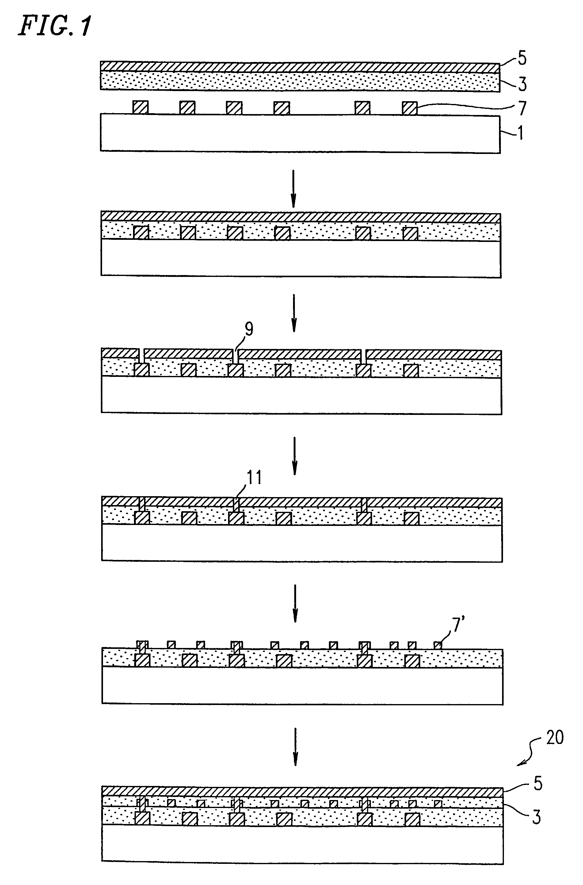
[0015]A problem to be solved by the present invention is to provide a multilayer structure suitable for production of a multilayer wiring board using a build-up method. More particularly, a problem to be solved by the present invention is to provide a multilayer structure having a high heat resistance, a narrow pitch wiring pattern, a small-diameter via, an insulating layer having a uniform thickness, an appropriately low coefficient of linear expansion, a high metal / polymer film adhesiveness, and excellent electrical properties and an excellent balance of physical properties for achieving a stable multilayer wiring board, and a multilayer wiring board using the same.

Problems solved by technology

However, it is pointed out that as superior properties are required for a build-up multilayer wiring board, several problems arise when using conventional copper foil with an insulating adhesive.
In particular, in a multilayer wiring board for which smaller size and lighter weight are required, a glass cloth-containing copper-clad laminate used as a core layer typically has a thickness of about 400 μm and a heavy weight due to the contained glass, and therefore is not a material suitable for reduction of size and weight.
If only copper foil with an insulating adhesive is used without using the glass cloth-containing copper-clad laminate to produce a build-up multilayer wiring board, it is possible to obtain one which has a smaller size and a lighter weight, but the resultant wiring board lacks rigidity, and also lacks package reliability due to a great coefficient of linear expansion derived from the insulating adhesive, and does not endure use.

Method used


Image

  • Multilayer structure and multilayer wiring board using the same
  • Multilayer structure and multilayer wiring board using the same
  • Multilayer structure and multilayer wiring board using the same

Examples


example 1

[0174](1) DMF and p-PDA having an equivalent weight of 1 and ODA having an equivalent weight of 1 were added to a separable flask, followed by stirring well at room temperature until the diamine compound was completely dissolved. Thereafter, the mixture was cooled on ice. TMHQ having an equivalent weight of 1 was added to the mixture, followed by stirring for 40 minutes while cooling. Thereafter, PMDA having an equivalent weight of 1 was dissolved in DMF, and was gradually added to the mixture, followed by stirring for 1 hour while cooling, to obtain a DMF solution of poly(amic acid). It should be noted that the amount of DMF used was equivalent to a monomer feed concentration of 18% by weight of the diamino compound and the aromatic tetracarboxylic acid compound.

[0175]10 g of acetic anhydride and 10 g of isoquinoline were added to 100 g of the above-described poly(amic acid) solution, followed by uniformly stirring. Thereafter, defoaming was performed. The mixture was flow-cast on ...

example 2

[0182]A heat resistant polyimide film having a copper thin film was obtained in the same manner as that of Examples 1(1) and (2), except that a poly(amic acid) solution flow-cast on a glass plate was dried at about 110° C. for about 5 minutes, the resultant poly(amic acid) gel film peeled off the glass plate, and was immersed in dihydroxytitaniumbislactate / 1-butanol solution having a titanium concentration of 400 ppm for 10 seconds, so that excess liquid drops were removed. The resultant polyimide film had a modulus of tensile elasticity of 6 GPa, a water absorption ratio of 1.2%, and a coefficient of linear expansion of 1.0×10⁻⁵ / ° C.

[0183]Varnish was prepared in a similar manner to Examples 1(3) and (4) flow-cast onto a surface of the resultant polyimide film, instead of the glass plate, followed by drying at 100° C. for 10 minutes, and then at about 150° C. for about 20 minutes, thereby obtaining a multilayer structure of the present invention comprising an adhesive layer having a...

example 3

[0186]A polyimide resin and a polyimide film were obtained in the same manner as that of Example 2, and a conductor layer was formed in the same manner as that of Example 2, except that a dihydroxytitaniumbislactate / 1-butanol solution having a titanium concentration of 1000 ppm was used. The resultant polyimide film had a modulus of tensile elasticity of 6 GPa, a water absorption ratio of 1.2%, and a coefficient of linear expansion of 1.0×10⁻⁵ / ° C. The multilayer structure had a conductor layer having an initial adhesive strength of 8 N / cm, and a satisfactory adhesive strength to a conductor, and is suitable as a material for a multilayer wiring board. Further, the thus-obtained multilayer structure was superimposed on the opposite surfaces of a circuit substrate having a circuit pattern on the opposite surfaces of a polyimide film thereof, where each adhesive layer thereof faces the circuit pattern surface, followed by lamination using a pressing apparatus where conditions for pres...


PUM

PropertyMeasurementUnit
water absorption ratioaaaaaaaaaa
dielectric breakdown voltageaaaaaaaaaa
adhesive strengthaaaaaaaaaa

Abstract

A multilayer structure comprising a conductor layer, an adhesive layer, and a polymer film layer interposed between the conductor layer and the adhesive layer. The multilayer structure can be used to provide a multilayer wiring board having excellent electrical properties and an excellent balance of physical properties, high heat resistance, a narrow pitch wiring pattern, a small-diameter via, uniform insulating layer thickness, an appropriately low coefficient of linear expansion, and stable adhesiveness between a metal and the polymer film. The polymer film layer may contain at least one repeating unit represented by formula (1) in the molecule. The present invention also provides a multilayer wiring board obtained from the multilayer structure.

Description

RELATED APPLICATIONS[0001]This application is a nationalization of PCT application PCT / JP01 / 03175 filed Dec. 4, 2001. This application claims priority from the PCT application and Japan Application Serial No. 2000-110199 filed Dec. 4, 2000; Japan Application Serial No. 2000-224861 filed Jul. 26, 2000.TECHNICAL FIELD[0002]The present invention relates to a multilayer structure comprising a conductor layer, a polymer film and an adhesive layer. More particularly, the present invention relates to a multilayer structure having excellent electrical properties and an excellent balance of physical properties, which can provide a multilayer wiring board has a high heat resistance, a narrow pitch wiring pattern, a small-diameter via, an insulating layer having a uniform thickness, an appropriately low coefficient of linear expansion, and a stable adhesiveness between a metal and a polymer film.BACKGROUND ART[0003]As electronic devices become smaller-sized, higher-performance, and more sophis...

Claims


Application Information

Patent Timeline
Patent Type & Authority Patents(United States)
IPC IPC(8): B32B15/08B32B27/28H05K1/03B32B27/06H05K3/38H05K3/46
CPCB32B27/06H05K3/4655Y10T428/2848H05K3/388H05K3/389H05K3/4652H05K2201/0129H05K2201/0154H05K2201/0195H05K2201/0209H05K2201/0239H05K2201/0358H05K2201/068H05K2203/121Y10T428/24917Y10T428/2804H05K3/386Y10T428/31681Y10T428/31692Y10T428/31721B32B27/00
Inventor ITOH, TAKASHIHARA, SHOJINAGANO, HIROSAKUNISHINAKA, MASARU
Owner KANEKA CORP
Learn More