Field-effect transistor, and integrated circuit device and switching circuit using the same
- Summary
- Abstract
- Description
- Claims
- Application Information
AI Technical Summary
Benefits of technology
Problems solved by technology
Method used
Image
Examples
embodiment 1
[0035](Embodiment 1)
[0036]A first embodiment of the present invention will be described with reference to the drawings.
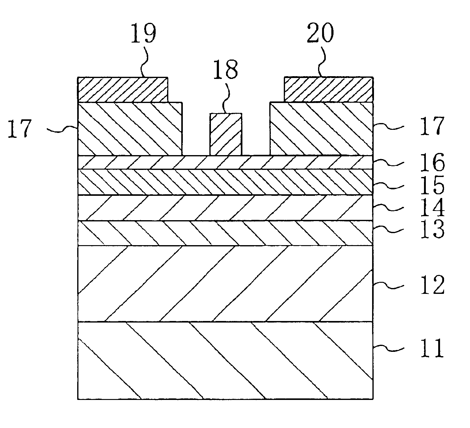
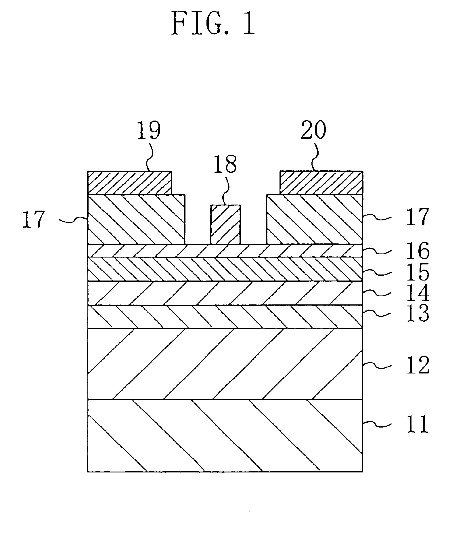
[0037]FIG. 1 is a structural cross sectional view showing a field-effect transistor according to a first embodiment of the present invention. As shown in FIG. 1, an approximately 500 nm-thick buffer layer 12 made of aluminum gallium arsenide (AlGaAs), an approximately 100 nm-thick barrier layer 13 made of n-type AlGaAs, an approximately 15 nm-thick channel layer 14 made of undoped indium gallium arsenide (InGaAs), an approximately 20 nm-thick carrier supply layer 15 made of n-type AlGaAs, an approximately 5 nm-thick Schottky layer 16 made of undoped indium gallium phosphate (InGaP) with a broken natural superlattice, an approximately 100 nm-thick cap layer 17 made of n-type-impurity-doped GaAs and having an opening at which the Schottky layer 16 is partly exposed are sequentially stacked, for example, on a compound semiconductor substrate 11 made of gallium arsenide...
embodiment 2
[0058](Embodiment 2)
[0059]A second embodiment of the present invention will be described hereinafter with reference to the drawing.
[0060]FIG. 3 shows the cross sectional structure of a field-effect transistor according to a second embodiment of the present invention. Referring to FIG. 3, the same numerals are given to the same members as in FIG. 1, and a description thereof is not given.
[0061]As shown in FIG. 3, a buffer layer 12, a barrier layer 13, a channel layer 14, a carrier supply layer 15, a Schottky layer 16, and a cap layer 107 are successively stacked on a compound semiconductor substrate 11. A gate electrode 18 is formed on a part of the Schottky layer 16 exposed at the recess opening of the cap layer 17 to serve as a Schottky electrode. Source and drain electrodes 19 and 20 are formed on the cap layer 17 placed to both sides of the gate electrode 18 to serve as ohmic electrodes.
[0062]A protective film 21 made of benzocyclobutene (BCB) is placed over the whole surface of ...
embodiment 3
[0067](Embodiment 3)
[0068]A third embodiment of the present invention will be described hereinafter with reference to the drawing.
[0069]FIG. 4 shows the cross sectional structure of an integrated circuit according to a third embodiment of the present invention. As shown in FIG. 4, an epitaxial layer 31 made of a compound semiconductor is formed on a compound semiconductor substrate 30 made of, for example, GaAs by crystal growth.
[0070]In the region denoted by 32 on the substrate 30 and the epitaxial layer 31, a field-effect transistor is formed to have the same structure as that of the first embodiment. A resistive element 33 and a capacitive element 34 are integrated on the substrate 30, thereby constructing a monolithic microwave integrated circuit (MMIC).
[0071]The resistive element 33 is composed of, for example, polysilicon (PS), tungsten silicide nitride (WSiN) or nickel chrome (NiCr). In this case, WSiN or NiCr is in particular preferable. The capacitive element 34 is composed...
PUM
 Abstract
Description
Claims
Application Information
 - R&D
- Intellectual Property
- Life Sciences
- Materials
- Tech Scout
- Unparalleled Data Quality
- Higher Quality Content
- 60% Fewer Hallucinations
Browse by: Latest US Patents, China's latest patents, Technical Efficacy Thesaurus, Application Domain, Technology Topic, Popular Technical Reports.
© 2025 PatSnap. All rights reserved.Legal|Privacy policy|Modern Slavery Act Transparency Statement|Sitemap|About US| Contact US: help@patsnap.com


