Semiconductor device and method for manufacturing same
a semiconductor and semiconductor technology, applied in the direction of coatings, transistors, chemical vapor deposition coatings, etc., can solve the problems of mos transistors, formed in semiconductor substrates, thermally affected and deteriorated, and achieve high crystallizing temperature and high quality
- Summary
- Abstract
- Description
- Claims
- Application Information
AI Technical Summary
Benefits of technology
Problems solved by technology
Method used
Image

Examples
first embodiment
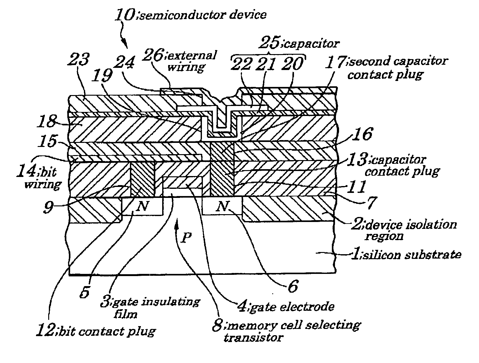
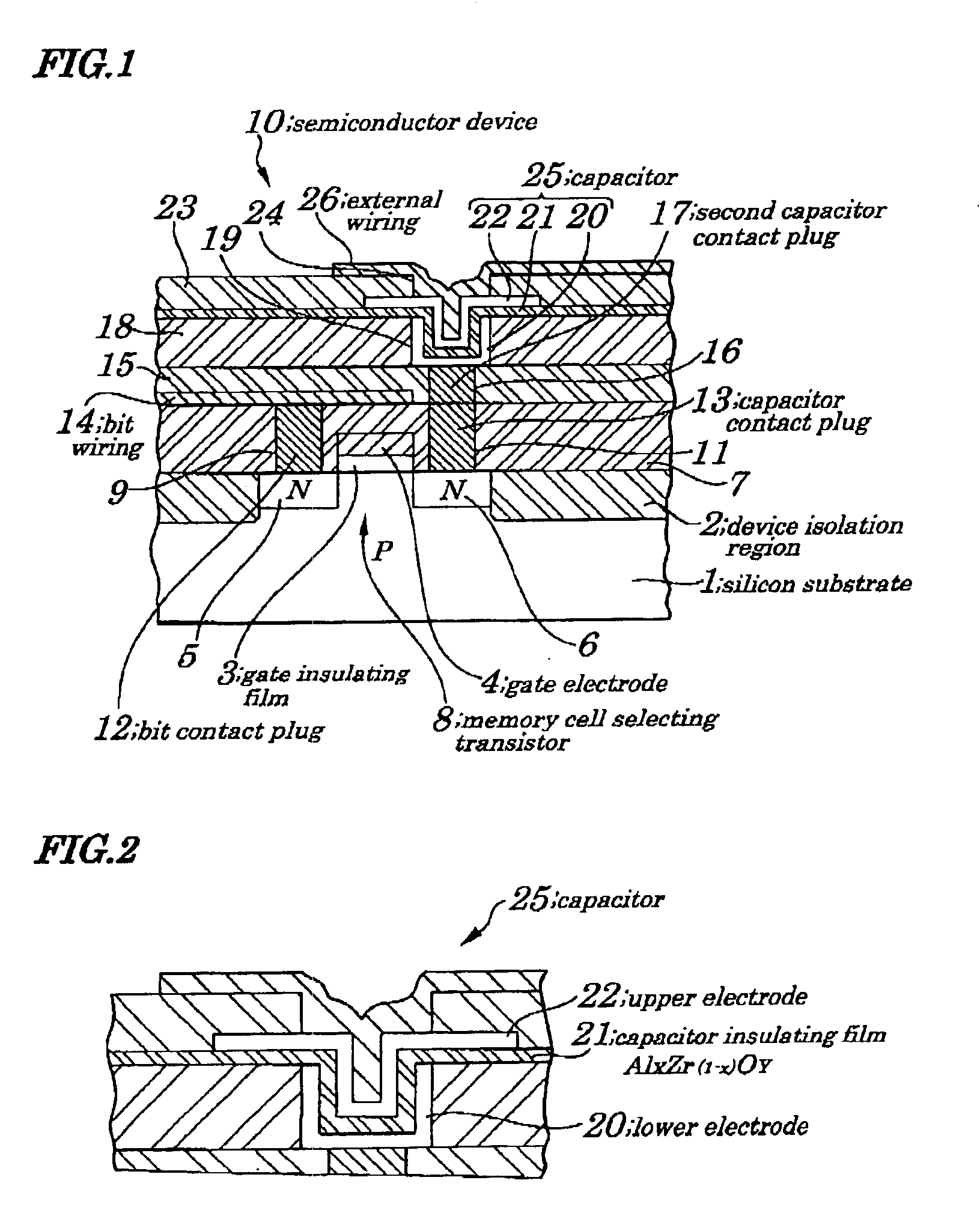
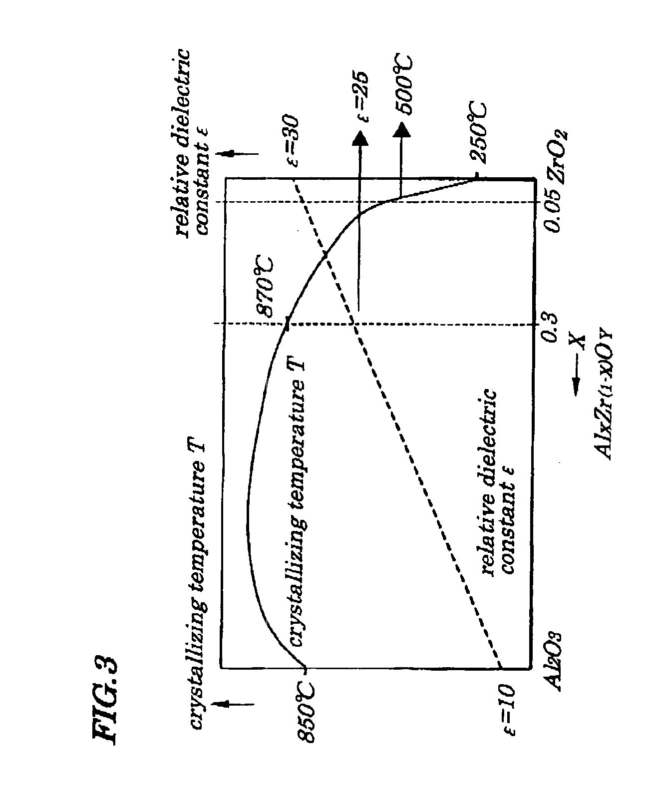
[0051]FIG. 1 is a cross-sectional view for schematically illustrating configurations of a semiconductor device according to a first embodiment of the present invention. FIG. 2 is an expanded cross-sectional view illustrating configurations of a capacitor serving as a main part of the semiconductor device according to the first embodiment. FIG. 3 is a diagram explaining a relative dielectric constant of a capacitor insulating film of the capacitor of the semiconductor device and an optimum range of a crystallizing temperature according to the first embodiment. FIGS. 4A to 4K are diagrams showing a manufacturing method for the semiconductor device, in order of processes, according to the first embodiment. FIG. 5 is a diagram briefly explaining a process for deposition of the capacitor insulating film employed in the manufacturing method for the semiconductor device according to the first embodiment. FIG. 6 is a diagram showing a sequence of deposition of the capacitor insulating film ...
second embodiment
[0081]A method for manufacturing semiconductor devices of a second embodiment differs greatly from that of the first embodiment in that, as a metal which can be used for forming crystalline dielectric, hafnium (Hf), instead of zirconium (Zr), is employed.
[0082]In the semiconductor device of the second embodiment, a capacitor insulating film is made of amorphous hafnium aluminate obtained by mixing amorphous aluminum oxide into hafnium oxide being crystalline dielectric, and having its composition of AlXHf(1-X)OY (0.05≦X≦0.3). That is, though, in a capacitor of a semiconductor device of the second embodiment, instead of amorphous zirconium aluminate used in the first embodiment, amorphous hafnium aluminate is used, relations among a composition ratio X of hafnium aluminate, relative dielectric constant “∈” of hafnium aluminate, and crystallizing temperature T are almost the same as those shown in FIG. 3 in the first embodiment, except that a dielectric constant (about 20) of hafnium ...
third embodiment
[0084]A method for manufacturing semiconductor devices of a third embodiment differs greatly from that of the first embodiment in that, as a metal which can be used for forming crystalline dielectric, a lanthanoid group element, instead of zirconium, is employed.
[0085]A capacitor insulating film of a capacitor in a semiconductor device of the third embodiment is made of amorphous lanthanoid aluminate obtained by having amorphous dielectric made of a lanthanoid group element contain amorphous aluminum oxide and having its composition of AlXRe(1-X)OY (“Re” denotes a lanthanoid group element, 0.05≦X≦0.3). The lanthanoide group element includes lanthanum (La), cerium (Ce), praseodymium (Pr), neodymium (Nd), promethium (Pm), samarium (Sm), europium (Eu), gadolinium (Gd), terbium (Tb), dysprosium (Dy), holmium (Ho), erbium (Er), thulium (Tm), ytterbium (Yb), and lutetium (Lu).
[0086]That is, though, in the capacitor of the semiconductor device of the third embodiment, instead of amorphous ...
PUM
| Property | Measurement | Unit |
|---|---|---|
| thickness | aaaaa | aaaaa |
| temperatures | aaaaa | aaaaa |
| thickness | aaaaa | aaaaa |
Abstract
Description
Claims
Application Information
 - R&D
- Intellectual Property
- Life Sciences
- Materials
- Tech Scout
- Unparalleled Data Quality
- Higher Quality Content
- 60% Fewer Hallucinations
Browse by: Latest US Patents, China's latest patents, Technical Efficacy Thesaurus, Application Domain, Technology Topic, Popular Technical Reports.
© 2025 PatSnap. All rights reserved.Legal|Privacy policy|Modern Slavery Act Transparency Statement|Sitemap|About US| Contact US: help@patsnap.com