Pattern forming method using developer containing organic solvent and rinsing solution for use in the pattern forming method
a technology of organic solvent and pattern forming method, which is applied in the field of pattern forming, can solve problems such as blob defects, and achieve the effect of high precision
- Summary
- Abstract
- Description
- Claims
- Application Information
AI Technical Summary
Benefits of technology
Problems solved by technology
Method used
Image
Examples
example 1
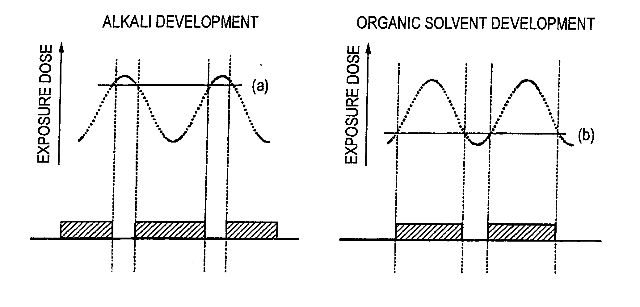
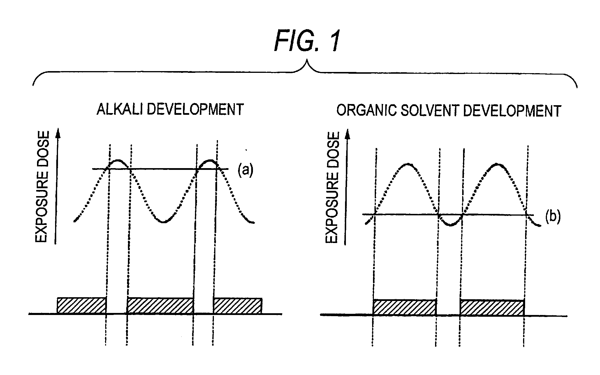
[0931]An organic antireflection film, ARC29A (produced by Nissan Chemical Industries, Ltd.), was applied on a silicon wafer and baked at 205° C. for 60 seconds to form a 86 nm-thick antireflection film, and Resist Composition Ar-01 shown in Table 4 was applied thereon and baked at 115° C. for 60 seconds (PB: Prebake) to form a 100 nm-thick resist film. The obtained wafer was subjected to pattern exposure through an exposure mask (line / space=1 / 1) by using an ArF excimer laser scanner (NA: 0.75). At this time, the area of exposure was set to 205 cm2 in total. Thereafter, the wafer was heated at 105° C. for 60 seconds (PEB: Post Exposure Bake), developed with an organic solvent-containing developer shown in Table 7 for 30 seconds (organic solvent-based development), rinsed with a rinsing solution shown in Table 7, and spun at a rotation speed of 4,000 rpm for 30 seconds to obtain a line-and-space (1:1) resist pattern having a line width of 150 nm.
examples 2 to 66 , 70 to 77 and 84 to 87
Examples 2 to 66, 70 to 77 and 84 to 87 and Comparative Examples 1 to 3
[0932]In the same manner as in the method of Example 1, line-and-space (1:1) resist patterns having a pitch of 300 nm and a line width of 150 nm of Examples 2 to 66, 70 to 77 and 84 to 87 and Comparative Examples 1 to 3 were obtained using Resist Compositions Ar-01 to Ar-67 and Ar-70 to Ar-77 shown in Tables 4 to 6 under the conditions shown in Tables 7 to 9.
[0933]In Tables 7 to 9, A1, A2, A3, B1 and the like indicative of the organic solvent-containing developer are the same as the symbols of solvents used in the preparation of resists above.
[0934]In the case where a solvent is shown in the column of Organic Solvent-containing Developer (2), this means that solvents shown in Organic Solvent Containing Developer (1) and Organic Solvent-Containing Developer (2) of Tables 7 to 9 were used in a solvent ratio (by mass) shown in Tables 7 to 9. Similarly, when a solvent is shown in the column of Rinsing Solution (2), t...
example 67
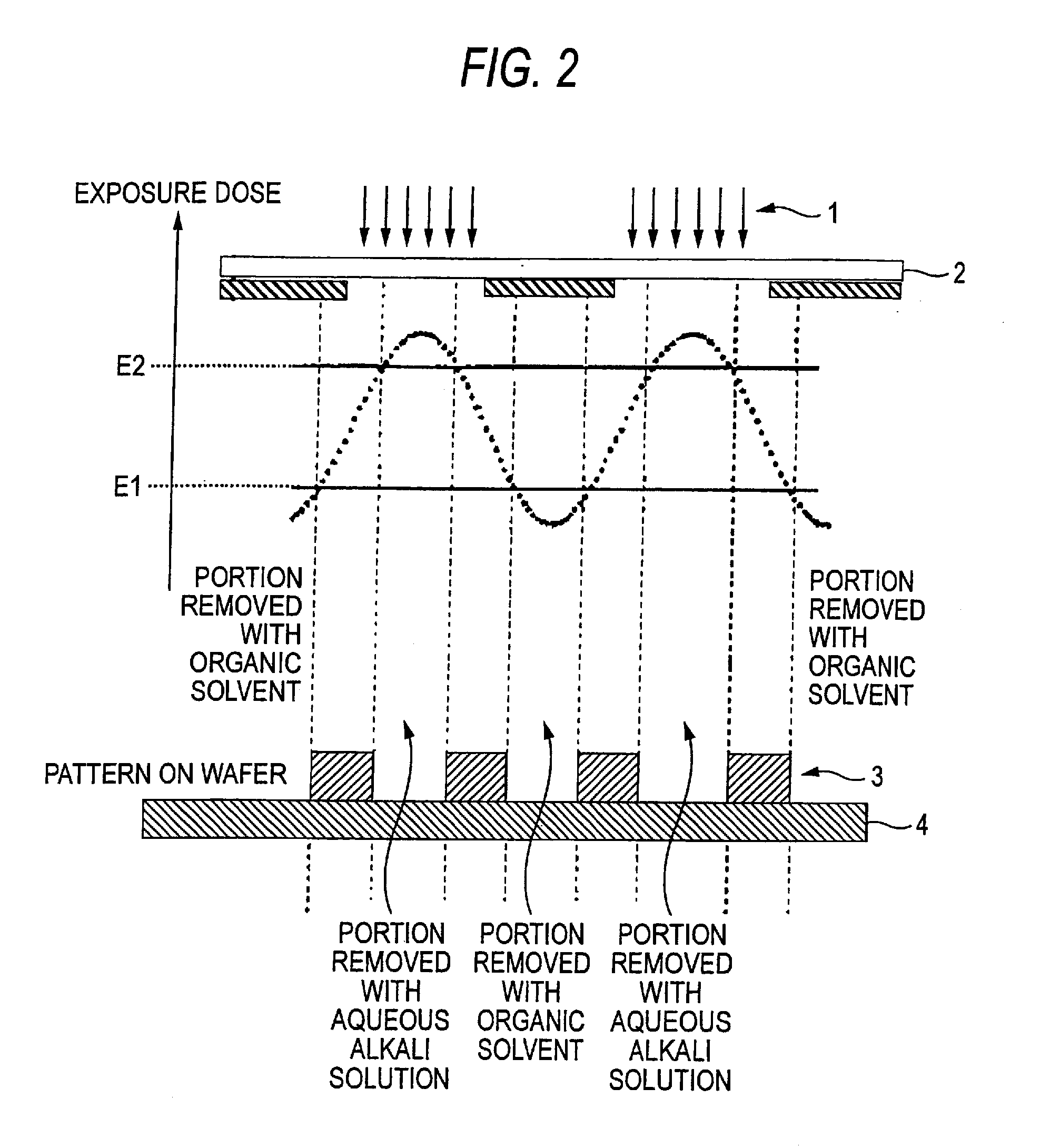
[0935]An organic antireflection film, ARC29A (produced by Nissan Chemical Industries, Ltd.), was applied on a silicon wafer and baked at 205° C. for 60 seconds to form a 78 nm-thick antireflection film, and Resist Composition Ar-67 was applied thereon and baked at 115° C. for 60 seconds (PB) to form a 150 nm-thick resist film. The obtained wafer was subjected to pattern exposure through an exposure mask (line / space=1 / 1) by using an ArF excimer laser scanner (NA: 0.75). At this time, the area of exposure was set to 205 cm2 in total. Thereafter, the wafer was heated at 85° C. for 60 seconds (PEB), developed with an aqueous tetramethylammonium hydroxide solution (2.38 mass %) (alkali developer) for 30 seconds (alkali development) and rinsed with pure water to obtain a pattern having a pitch of 600 nm and a line width of 450 nm. Subsequently, the wafer was developed with an organic solvent-containing developer shown in Table 9 for 30 seconds (organic solvent-based development), rinsed w...
PUM
| Property | Measurement | Unit |
|---|---|---|
| carbon number | aaaaa | aaaaa |
| wavelength | aaaaa | aaaaa |
| boiling point | aaaaa | aaaaa |
Abstract
Description
Claims
Application Information
 - R&D
- Intellectual Property
- Life Sciences
- Materials
- Tech Scout
- Unparalleled Data Quality
- Higher Quality Content
- 60% Fewer Hallucinations
Browse by: Latest US Patents, China's latest patents, Technical Efficacy Thesaurus, Application Domain, Technology Topic, Popular Technical Reports.
© 2025 PatSnap. All rights reserved.Legal|Privacy policy|Modern Slavery Act Transparency Statement|Sitemap|About US| Contact US: help@patsnap.com


