
Pattern forming method, resist composition for multiple development used in the pattern forming method, developer for negative development used in the pattern forming method, and rinsing solution for negative development used in the pattern forming method

a pattern forming and composition technology, applied in the field of pattern forming methods, can solve the problems of reducing optical contrast, inability to obtain sufficient exposure margin or focal depth, etc., and achieve the effect of high precision and integrated electronic technology

Active Publication Date: 2008-08-07
FUJIFILM CORP
View PDF92 Cites 382 Cited by
  • Summary
  • Abstract
  • Description
  • Claims
  • Application Information

AI Technical Summary

Benefits of technology

[0022]An object of the present invention is to solve those problems and provide a method for stably forming a high-precision fine pattern to produce a highly integrated electronic device with high precision.

Problems solved by technology

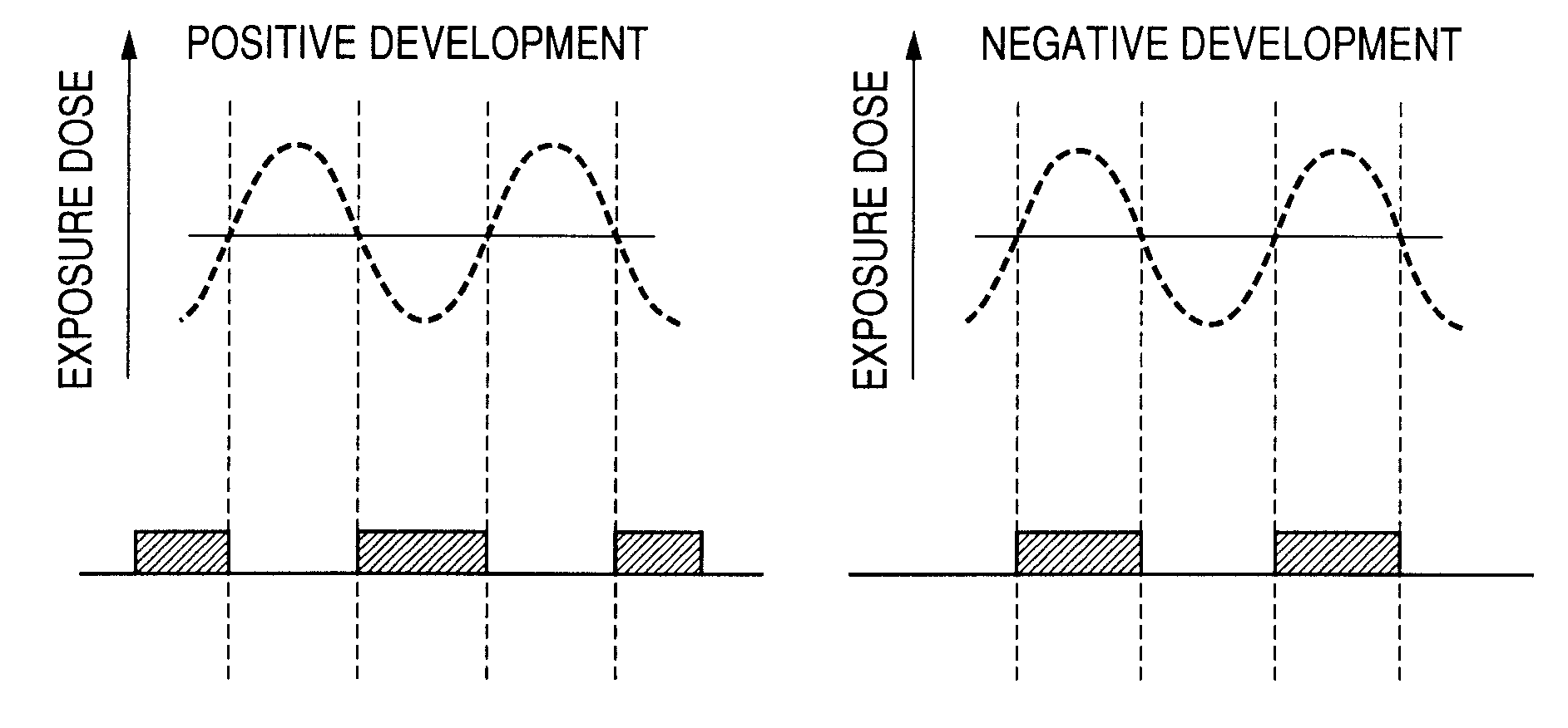
With the progress to finer dimension, the conventional exposure system comes to encounter a problem that lights irradiated on adjacent patterns interfere each other to decrease the optical contrast.
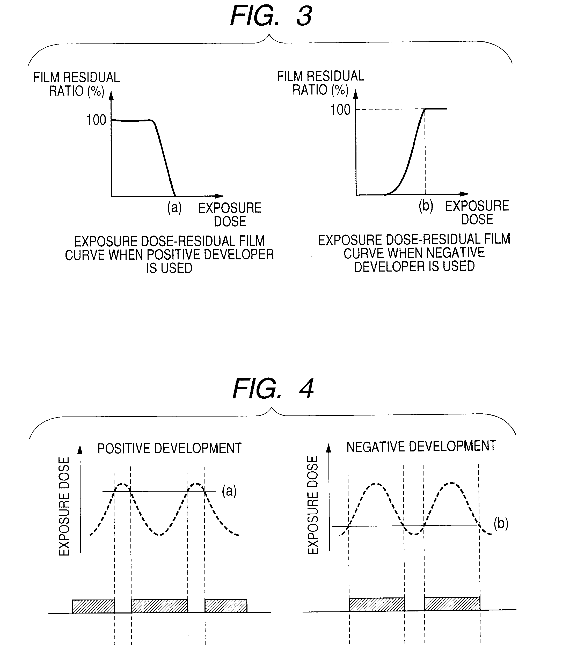
However, in these double exposure systems, the pattern formation needs to be performed in the vicinity of resolution limit of the resist and therefore, if the pattern formation is performed by merely applying the conventional resist composition to the conventional resist process, there arises a problem that sufficient exposure margin or focal depth cannot be obtained.

Method used


Image

  • Pattern forming method, resist composition for multiple development used in the pattern forming method, developer for negative development used in the pattern forming method, and rinsing solution for negative development used in the pattern forming method
  • Pattern forming method, resist composition for multiple development used in the pattern forming method, developer for negative development used in the pattern forming method, and rinsing solution for negative development used in the pattern forming method
  • Pattern forming method, resist composition for multiple development used in the pattern forming method, developer for negative development used in the pattern forming method, and rinsing solution for negative development used in the pattern forming method

Examples


example 1

[0681]An organic antireflection film, ARC29A (produced by Nissan Chemical Industries, Ltd.), was coated on a silicon wafer by a spin coater and baked at 205° C. for 60 seconds to form a 78-nm antireflection film, and a commercially available product, FAiRS-9101A12 (an ArF positive resist composition, produced by FUJIFILM Electronic Materials Co., Ltd.), was coated thereon and baked at 100° C. for 60 seconds to form a 150-nm resist film. The obtained wafer was subjected to pattern exposure at 25 [mJ / cm2] by using an ArF excimer laser scanner (NA: 0.75). Thereafter, the resist film was heated at 120° C. for 60 seconds, developed with butyl acetate (negative developer) for 30 seconds (negative development), and rinsed with decane for 30 seconds to obtain a resist pattern having a pitch of 200 nm and a line width of 100 nm.

synthesis example 1

Synthesis of Resin (A1)

[0682]Under a nitrogen stream, 8.4 g of methyl isobutyl ketone was charged into a three-neck flask and heated at 80° C. Thereto, a solution obtained by dissolving 9.4 g of 2-cyclohexylpropan-2-yl methacrylate, 4.7 g of 3-hydroxy-1-adamantyl methacrylate, 6.8 g of β-methacryloyloxy-γ-butyrolactone and azobisisobutyronitrile corresponding to 6 mol % based on the entire monomer amount, in 75.3 g of methyl isobutyl ketone was added dropwise over 6 hours. After the completion of dropwise addition, the reaction was further allowed to proceed at 80° C. for 2 hours. The resulting reaction solution was left standing to cool and then, poured in 720 ml of heptane / 80 ml of ethyl acetate, and the powder precipitated was collected by filtration and dried, as a result, 18.3 g of Resin (A1) was obtained. The weight average molecular weight of the obtained resin was 9,300 and the dispersity (Mw / Mn) was 1.98.

Positive Resist Composition (A):

[0683]A solution having a solid conten...

example 2

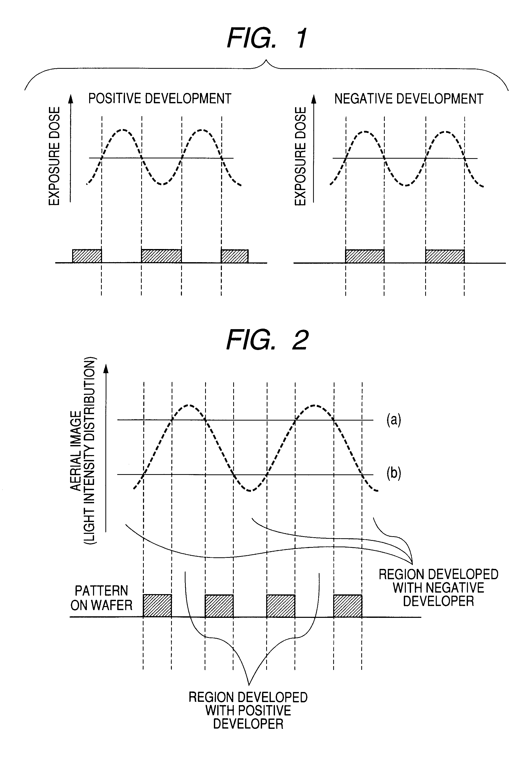
[0697]An organic antireflection film, ARC29A (produced by Nissan Chemical Industries, Ltd.), was coated on a silicon wafer and baked at 205° C. for 60 seconds to form a 78-nm antireflection film, and Positive Resist Composition (B) prepared above was coated thereon by a spin coater and baked at 100° C. for 60 seconds to form a 150-nm resist film. The obtained wafer was subjected to pattern exposure using an ArF excimer laser scanner (NA: 0.75). Thereafter, the resist film was heated at 120° C. for 60 seconds, developed with an aqueous tetramethylammonium hydroxide solution (2.38 mass %) (positive developer) for 30 seconds (positive development), and rinsed with pure water for 30 seconds to obtain a pattern having a pitch of 1,000 nm and a line width of 750 nm. Furthermore, the resist film was developed with a 2:3 (by mass) solution of butyl acetate / 2-hexanol (negative developer) for 30 seconds (negative development) to obtain a 250-nm (1:1) resist pattern.


PUM

PropertyMeasurementUnit
wavelengthaaaaaaaaaa
solubilityaaaaaaaaaa
thresholdaaaaaaaaaa

Abstract

A pattern forming method, including: (A) coating a substrate with a positive resist composition of which solubility in a positive developer increases and solubility in a negative developer decreases upon irradiation with actinic rays or radiation, so as to form a resist film; (B) exposing the resist film; and (D) developing the resist film with a negative developer; a positive resist composition for multiple development used in the method; a developer for use in the method; and a rinsing solution for negative development used in the method.

Description

BACKGROUND OF THE INVENTION[0001]1. Field of the Invention[0002]The present invention relates to a pattern forming method for use in the process of producing a semiconductor such as IC, in the production of a circuit board for liquid crystal, thermal head and the like, and in the lithography process of other photo applications; a positive resist composition for multiple development used in the pattern forming method; a developer for negative development used in the pattern forming method; and a rinsing solution for negative development used in the pattern forming method. More specifically, the present invention relates to a pattern forming method suitable for exposure with an ArF exposure apparatus using a light source that emits far ultraviolet light at a wavelength of 300 nm or less or with an immersion-type projection exposure apparatus; a positive resist composition for multiple development used in the pattern forming method; a developer for negative development used in the patt...

Claims


Application Information

Patent Timeline
Patent Type & Authority Applications(United States)
IPC IPC(8): G03F7/00G03F7/004
CPCG03F7/2024G03F7/32G03F7/2002G03F7/039G03F7/40Y10T428/24802G03F7/0392G03F7/0397G03F7/325G03F7/30B32B3/10G03F7/0382G03F7/26H01L21/0274G03F7/038G03F7/16G03F7/0035G03F7/0758G03F7/095G03F7/322
Inventor TSUBAKI, HIDEAKIKANNA, SHINICHI
Owner FUJIFILM CORP
Learn More