
Capacitive substrate and method of making same

Inactive Publication Date: 2007-11-29
TTM TECH NORTH AMERICA LLC
View PDF23 Cites 22 Cited by
  • Summary
  • Abstract
  • Description
  • Claims
  • Application Information

AI Technical Summary

Benefits of technology

[0036]It is, therefore, a primary object of the present invention to enhance the circuitized substrate art by providing a circuitized substrate having the advantageous features taught herein.
[0037]It is another object of the invention to provide a method of making such a circuitized substrate which can be accomplished in a relatively facile manner and at relatively low costs.

Problems solved by technology

The discrete passive devices occupy a high percentage of the surface area of the completed substrate, which is undesirable from a future design aspect because of the increased need and demand for miniaturization in today's substrates and products containing same art.
Some of the patents listed below, particularly U.S. Pat. No. 5,162,977, mention use of various materials for providing desired capacitance levels under this formula, and many mention or suggest problems associated with the methods and resulting materials used to do so.
That is, the resulting PCB still requires the utilization of external devices thereon, and thus does not afford the PCB external surface area real estate savings mentioned above which are desired and demanded in today's technology.
Although the pre-fired and ground dielectric formulations produced by solid phase reactions are acceptable for many electrical applications, these suffer from several disadvantages.
First, the milling step serves as a source of contaminants, which can adversely affect electrical properties.
Second, the milled product consists of irregularly shaped fractured aggregates which are often too large in size and possess a wide particle size distribution, 500-20,000 nm.
Consequently, films produced using these powders are limited to thicknesses greater than the size of the largest particle.
Thirdly, powder suspensions or composites produced using pre-fired ground ceramic powders typically must be used immediately after dispersion, due to the high sedimentation rates associated with large particles.
It is thus clear that methods of making PCBs which rely on the advantageous features of using nano-powders as part of the PCB's internal components or the like, such as those described in selected ones of the above patents, possess various undesirable aspects which are detrimental to providing a PCB with optimal functioning capabilities when it comes to internal capacitance or other electrical operation.

Method used


Image

  • Capacitive substrate and method of making same
  • Capacitive substrate and method of making same
  • Capacitive substrate and method of making same

Examples


example one

[0068]BaTiO3-thin films were prepared from a 0.5 molar aqueous acetate solution of Ba(CH3COO)2 and Ti(OC2H5)4. The films were deposited on glass substrates and dried successively at 150° and 450° C. to remove all the organics. The films were then laser annealed at various fluences (energy densities) for one to 300 pulses per area. Additional post annealing (600° C. in air) was used to generate different crystalline phases in the laser-annealed spots. A second electrical conductor was then formed using a sputtering operation atop the cured film using a mask normally used for such sputtering operations. The resulting capacitance density of the formed capacitor measured about 3000-5000 pico-Farads (pF) / square millimeter at one Mega-Hertz (MHz). The following Table illustrates how a change of capacitance will occur with such laser anneal

TABLECapacitanceLaser annealingPost annealing(pF / mm2)Blank600 degree C. for10001 hour250 mJ / cm2 for 50600 degree C. for3000pulses1 hour370 mJ / cm2 for 50...

example two

[0069]BaTiO3 powders (40 grams) were mixed with a solution containing two grams of n-phenylaminopropyltrimethoxy silane, ethanol (95 ml) and water (5 ml). The white suspension formed was ultrasonicated for five minutes and then stirred at 70° C. for one hour. The product was collected by centrifugation, washed with ethanol (120 ml×2) and vacuum dried. Epoxy based nanocomposites were prepared by mixing appropriate amounts of the organically modified BaTiO3 powder, bisphenol A epoxy resin (Mn˜377), dicyandiamide, and 2-methylimidazole in methylpyrrolidone (NMP). The mixture was stirred and ultrasonicated for five minutes to homogenize the dispersion of BaTiO3. Composite thin films were deposited on Cu substrates, which served as the bottom electrode. The films were first dried at 75° C. for one hour followed by curing in a vacuum oven at 170° C. for fifteen hours. The films were then laser annealed at fluences (energy densities) 50-100 mille Jules (mJ) / square centimeter for one to 300...

example three

[0070]38.5 grams of an epoxy novolac resin (sold under the product name “LZ 8213” from Huntsman, Salt Lake City, Utah), containing about 35 wt % methyl ethyl ketone and 6.5 gm of a phenoxy resin (sold under the product name “PKHC” from Phenoxy Associates, Rock Hill, S.C.), containing 50 wt % methyl ethyl ketone, were mixed together with 100 gm of barium titanate (BaTiO3) powder (available from Cabot Corporation, Boyertown, Pa.), the barium titanate including fifty grams with a mean particle size of 0.065 micron and surface area of about 16 m2 / gm, and fifty grams with a mean particle size of 0.12 micron and surface area of about 8.2 m2 / gm. This mixture was mixed with thirteen grams of propylene glycol methyl ether acetate and twelve grams of methyl ethyl ketone and ball milled for three days. A thin film (about 2.5 microns thick) of this mixed composite was then deposited on a copper substrate and dried at approximately 140° C. for three minutes in an oven to remove residual organic ...


PUM


Abstract

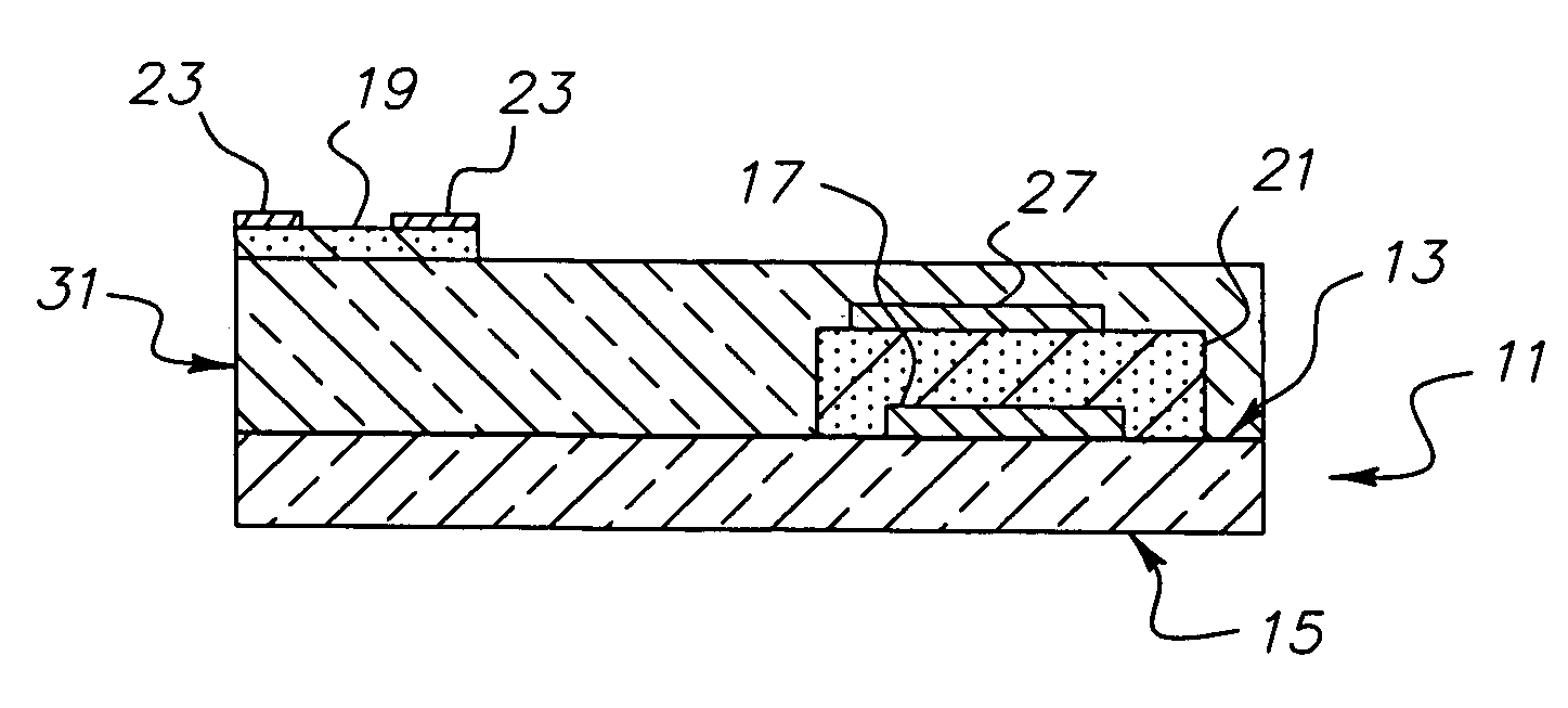
A capacitive substrate and method of making same in which first and second glass layers are used. A first conductor is formed on a first of the glass layers and a capacitive dielectric material is positioned over the conductor. The second conductor is then positioned on the capacitive dielectric and the second glass layer positioned over the second conductor. Conductive thru-holes are formed to couple to the first and second conductors, respectively, such that the conductors and capacitive dielectric material form a capacitor when the capacitive substrate is in operation.

Description

TECHNICAL FIELD[0001]The present invention relates to methods of forming capacitors within circuitized substrates such as printed circuit boards, chip carriers and the like, and to products including such internal capacitors as part thereof.CROSS-REFERENCE TO CO-PENDING APPLICATIONS[0002]In Ser. No. 10 / 900,385, entitled “Circuitized Substrate With Internal Organic Memory Device, Method Of Making Same, Electrical Assembly Utilizing Same, and Information Handling System Utilizing Same” and filed Jul. 28, 2004, there is defined a circuitized substrate comprised of at least one layer of dielectric material having an electrically conductive pattern thereon. At least part of the pattern is used as the first layer of an organic memory device which further includes at least a second dielectric layer over the pattern and a second pattern aligned with respect to the lower part for achieving several points of contact to thus form the device. The substrate is preferably combined with other diel...

Claims


Application Information

Patent Timeline
IPC IPC(8): H01L21/8242
CPCH01L27/12H01L28/40H05K1/0306H05K1/162H05K2203/013H05K3/4667H05K2201/0187H05K2201/09509H05K3/125
Inventor DAS, RABINDRA N.EGITTO, FRANK D.LAUFFER, JOHN M.LIN, HOW T.MARKOVICH, VOYA R.
Owner TTM TECH NORTH AMERICA LLC
Learn More