
Non-flaking capacitor material, capacitive substrate having an internal capacitor therein including said non-flaking capacitor material, and method of making a capacitor member for use in a capacitive substrate

a non-flaking capacitor and capacitive substrate technology, applied in the field of capacitors, can solve the problems of loss of continuity in the internal wall metal deposit, inability to afford the pcb external surface area real estate savings, and fibrous materials occupying a relatively significant portion of the substrate's total volume, so as to improve the circuitized substrate art

Inactive Publication Date: 2007-08-02
I3 ELECTRONICS
View PDF32 Cites 31 Cited by
  • Summary
  • Abstract
  • Description
  • Claims
  • Application Information

AI Technical Summary

Benefits of technology

[0047] It is another object of the invention to provide a method of making such a capacitor member which can be accomplished in a relatively facile manner and at relatively low costs.

Problems solved by technology

Typically, these discrete passive devices occupy a high percentage of the surface area of the completed multi-layered substrate, which is obviously undesirable from a future design perspective due to the ever-present demand for miniaturization.
With respect to the following patents, many mention or suggest problems associated with the methods and resulting materials used to do so.
That is, the resulting PCB still requires the utilization of external devices thereon, and thus does not afford the PCB external surface area real estate savings mentioned above which are desired and demanded in today's technology.
Such fibrous materials occupy a relatively significant portion of the substrate's total volume, a disadvantage especially when attempting to produce highly dense numbers of thru-holes and very fine line circuitry to meet new, more stringent design requirements.
If the glass is not removed, a loss of continuity might occur in the internal wall metal deposit.
In addition, both continuous and semi-continuous glass fibers add weight and thickness to the overall final structure, yet another disadvantage associated with such fibers.
Additionally, since lamination is typically at a temperature above 150 degrees C., the resinous portion of the laminate usually shrinks during cooling to the extent permitted by the rigid copper cladding, which is not the case for the continuous strands of fiberglass or other continuous reinforcing material used.
The strands thus take on a larger portion of the substrate's volume following such shrinkage and add further to complexity of manufacture in a high-density product.
Obviously, this problem is exacerbated as feature sizes (line widths and thicknesses, and thru-hole diameters) decrease.
Consequently, even further shrinkage may occur.
The shrinkage, possibly in part due to the presence of the relatively large volume percentage of continuous or semi-continuous fiber strands in the individual layers used to form a final product possessing many such layers, may have an adverse affect on dimensional stability and registration between said layers, adding even more problems for the PCB manufacturer.
Glass fiber presence, especially woven glass fibers, also substantially impairs the ability to form high quality, very small thru-holes using a laser.
This wide variation in encountered glass density leads to problems obtaining the proper laser power for each thru-hole and may result in wide variations in thru-hole quality, obviously unacceptable by today's very demanding manufacturing standards.
Glass fiber presence also often contributes to an electrical failure mode known as CAF growth.
CAF (cathodic / anodic filament) growth often results in an electrical shorting failure which occurs when dendritic metal filaments grow along an interface (typically a glass fiber / epoxy resin interface), creating an electrical path between two features which should remain electrically isolated.
While the use of glass mattes composed of random discontinuous chopped fibers (in comparison to the longer fibers found in continuous structures) can largely abate the problem of inadequate laser drilled thru-hole quality, such mattes still contain fibers with substantial length compared to internal board feature spacing and, in some cases, offer virtually no relief from the problem of this highly undesirable type of growth.
Use of pre-fired and ground ceramic powders in the dielectric layer, including as substitutes for the above glass fibers, also generally poses obstacles for the formation of thru-holes between conductive layers of a PCB.
Another problem associated with pre-fired ceramic nano-powders is the ability for the dielectric layer to withstand substantial voltage without breakdown occurring across the layer.
This is even further undesirable because, as indicated by the equation cited above, greater planar capacitance may also be achieved by reducing the thickness of the dielectric layer.
Although the pre-fired and ground dielectric formulations produced by solid phase reactions are acceptable for many electrical applications, these suffer from several disadvantages.
First, the milling step serves as a source of contaminants, which can adversely affect electrical properties.
Second, the milled product consists of irregularly shaped fractured aggregates which are often too large in size and possess a wide particle size distribution, 500-20,000 nm.
Consequently, films produced using these powders are limited to thicknesses greater than the size of the largest particle.
Thirdly, powder suspensions or composites produced using pre-fired ground ceramic powders typically must be used immediately after dispersion, due to the high sedimentation rates associated with large particles.
It is thus clear that methods of making PCBs which rely on the advantageous features of using nano-powders as part of the PCB's internal components or the like, such as those described in selected ones of the above patents, possess various undesirable aspects which are detrimental to providing a PCB with optimal functioning capabilities when it comes to internal capacitance or other electrical operation.

Method used


Image

  • Non-flaking capacitor material, capacitive substrate having an internal capacitor therein including said non-flaking capacitor material, and method of making a capacitor member for use in a capacitive substrate
  • Non-flaking capacitor material, capacitive substrate having an internal capacitor therein including said non-flaking capacitor material, and method of making a capacitor member for use in a capacitive substrate
  • Non-flaking capacitor material, capacitive substrate having an internal capacitor therein including said non-flaking capacitor material, and method of making a capacitor member for use in a capacitive substrate

Examples


example one

[0083] 38.5 grams (gm) of epoxy novolac resin (e.g., one sold under product designation “LZ 8213” by Huntsman, having a business location at 500 Huntsman Way, Salt Lake City, Utah) containing about 35 percent by weight methyl ethyl ketone, and catalyzed with about 0.015 parts per hundred (PPH) of 2-methyl-imidazole and 12.8 gm of a high molecular weight, reactive thermoplastic phenoxy resin (e.g., the aforementioned one sold under the product name “PKHS-40” by the Inchem Corporation) containing 60 percent by weight methyl ethyl ketone, were mixed together with 100 gm of barium titanate (BaTiO3) powder (available from Cabot Corporation, having a business location in Boyertown, Pa.). The barium titanate powder included a mean particle size of 0.12 microns and a surface area of 8.2 m2 / gm. Also mixed in with this composition was 20 gm of methyl ethyl ketone. The composition was ball milled for one day, after which a thin coating of this well dispersed composition was wire-rod coated on ...

example two

[0084] 50 gm of epoxy novolac resin (e.g., the “LZ 8213” above by Huntsman, containing about 35 percent by weight methyl ethyl ketone and catalyzed with about 0.015 PPH of 2-methyl-imidazole, and 19.2 gm of the high molecular weight, reactive thermoplastic phenoxy resin “PKHS-40” (containing 60 percent by weight methyl ethyl ketone), were mixed together with 111 gm of barium titanate (BaTiO3) powder from Cabot Corporation having the same mean particle size and surface area as in Example One (0.12 microns and 8.2 m2 / gm, respectively). Also mixed in with this composition was 20 gm of methyl ethyl ketone. As also in Example One, the composition was ball milled for one day, after which a thin coating of this mixed composition was deposited on a copper substrate (a copper foil) and dried at about 130 degrees C. for three minutes in a standard convection oven. This heating for this time period also served to substantially remove all residual organic solvents. Following removal and cooling...


PUM

PropertyMeasurementUnit
particle sizeaaaaaaaaaa
surface areaaaaaaaaaaa

Abstract

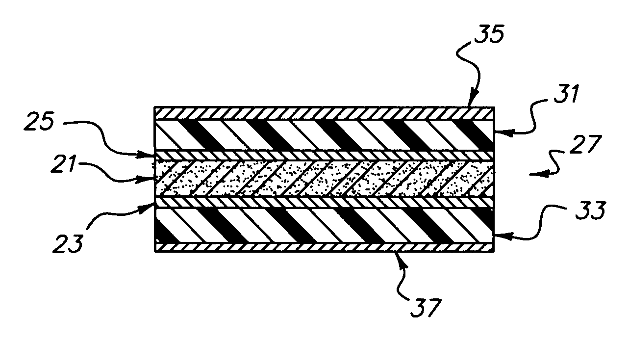
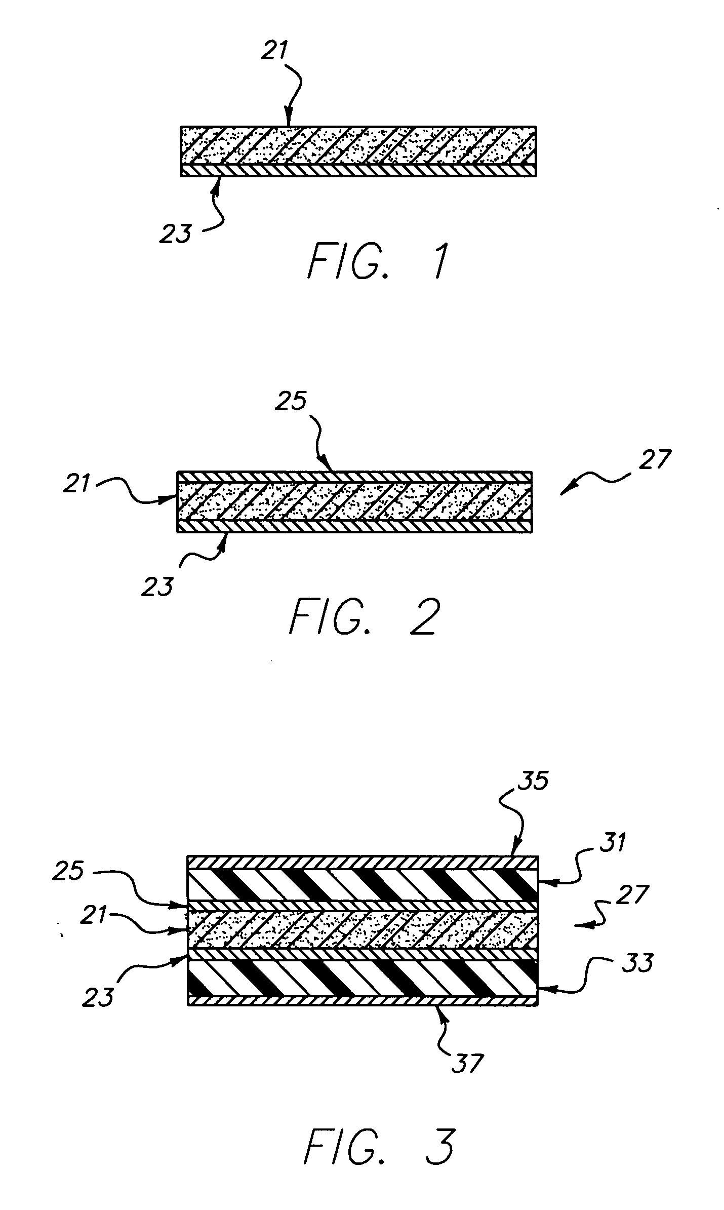
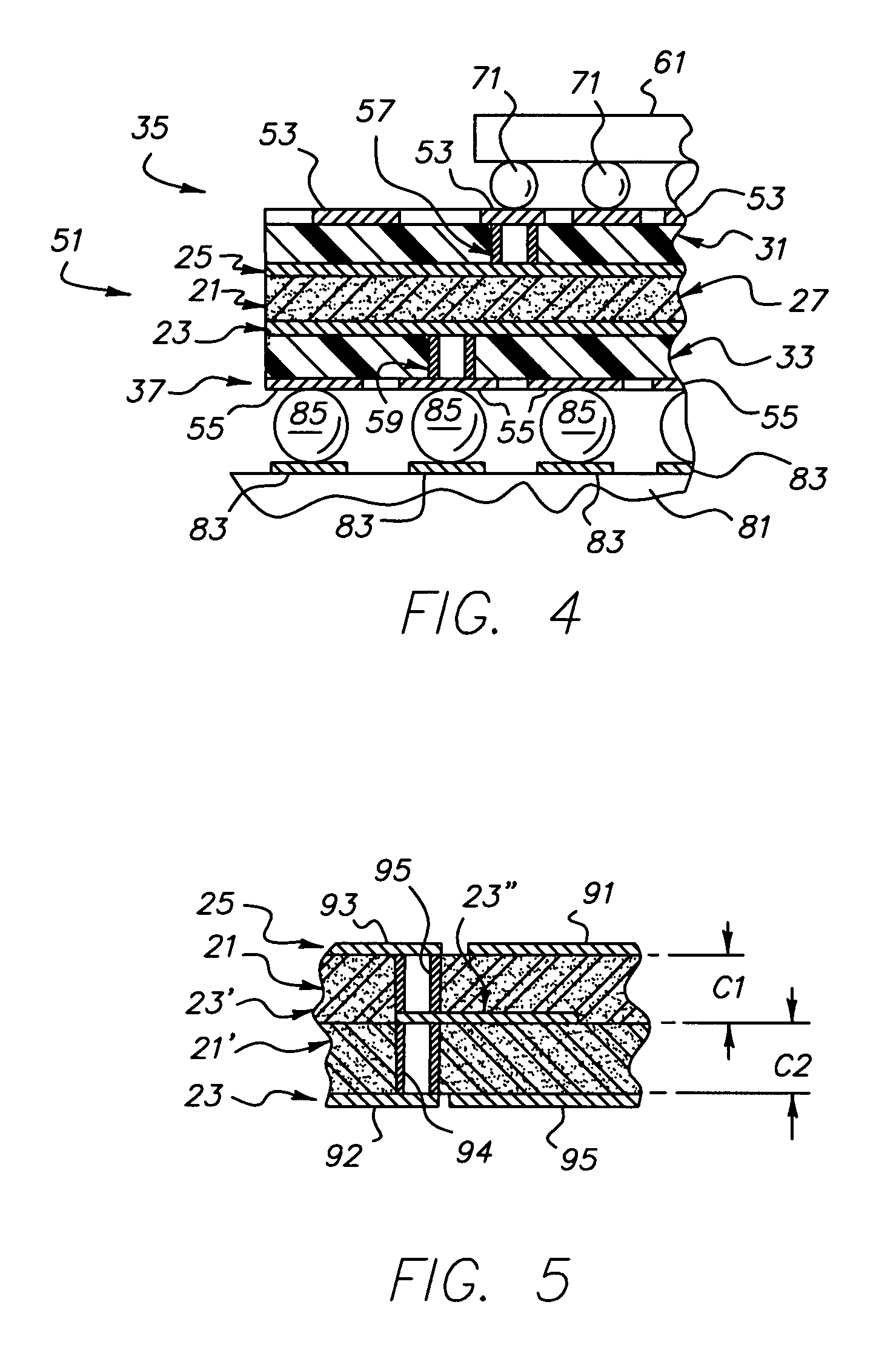
A capacitor material including a thermosetting resin (e.g., epoxy resin), a high molecular mass flexibilizer (e.g., phenoxy resin), and a quantity of nano-particles of a ferroelectric ceramic material (e.g., barium titanate), the capacitor material not including continuous or semi-continuous fibers (e.g., fiberglass) as part thereof. The material is adapted for being positioned in layer form on a first conductor member and heated to a predetermined temperature whereupon the material will not possess any substantial flaking characteristics. A second conductor member may then be positioned on the material to form a capacitor member, which then may be incorporated within a substrate to form a capacitive substrate. Electrical components may be positioned on the substrate and capacitively coupled to the internal capacitor.

Description

TECHNICAL FIELD [0001] The present invention relates to capacitors and particularly to internal capacitors for use within circuitized substrates such as printed circuit boards, chip carriers and the like, to products including such internal capacitors as part thereof, and to methods of making such capacitors. CROSS REFERENCE TO PREVIOUS AND CURRENT CO-PENDING APPLICATIONS OF THE ASSIGNEE [0002] In Ser. No. 11 / 031,074, entitled “Capacitor Material With Metal Component For Use In Circuitized Substrates, Circuitized Substrate Utilizing Same, Method of Making Said Circuitized Substrate, and Information Handling System Utilizing Said Circuitized Substrate” and filed Jan. 10, 2005, there is defined a material for use as part of an internal capacitor within a circuitized substrate in which the material includes a polymer resin and a quantity of nano-powders including a mixture of at least one metal component and at least one ferroelectric ceramic component, the ferroelectric ceramic compon...

Claims


Application Information

Patent Timeline
Patent Type & Authority Applications(United States)
IPC IPC(8): H01G4/228
CPCH01G4/206H01G4/232H01G4/33Y10T29/43H05K2201/0209H05K2201/0257H05K2201/09309H05K1/162
Inventor DAS, RABINDRA N.LAUFFER, JOHN M.MARKOVICH, VOYA R.PAPATHOMAS, KOSTAS I.
Owner I3 ELECTRONICS
Learn More