
Novolatile semiconductor memory device and manufacturing process of the same

Inactive Publication Date: 2005-06-09
ASAHI GLASS CO LTD +1
View PDF13 Cites 106 Cited by
  • Summary
  • Abstract
  • Description
  • Claims
  • Application Information

AI Technical Summary

Benefits of technology

[0022] The present invention provides a nonvolatile semiconductor memory device comprising a source region and a drain region formed on a surface of a semiconductor substrate; a tunnel insulating film formed in contact with a channel forming region so as to connect the source region and the drain region, the channel forming region being sandwiched between the source region and the drain region; a charge retention layer formed so as to be adjacent to the tunnel insulating film; a gate insulating film formed so as to be adjacent to the charge retention layer, and a co

Problems solved by technology

However, because DRAMs have volatility characteristic (that is, stored data are lost when power supply from an external power source is stopped) that is fatal to a memory, the DRAMs have caused, e.g., problems that it takes much time to start up a personal computer employing a DRAM, and that prepared data are lost by, e.g., a sudden stop of power supply or failure to store the data.
On the other hand, although hard disk systems do not have volatility characteristic of data, these systems have caused problems of slow writing and reading speed and relatively high power consumption.
However, since MRAM cell composes a transistor and a TMR (Tunnel Magneto Resistive) element, which makes disadvantageous in manufacturing cost due to its relatively complicated cell structure, and MRAM also has to employ a ferromagnetic material involving many technical problems in terms of process.
And, more importantly, there is a problem that the manufacturing technology for TMR element with minimized dispersions in characteristics is difficult to be established.
The hot electron injection is fast in terms of charge transfer speed, but low in terms of charge injection efficiency (proportion of an injecting current to a supply current).
And then the Fowler-Nordheim tunneling current at discharging is high in terms of the charge injection efficiency, but slow in terms of the charge transfer speed.
Consequently, both require much time for rewriting.
For this reason, it has been difficult to replace high-speed memory, such as DRAM, by flash memory, since, although flash memory are relatively easy to increase capacity and reduce costs, the application of the flash memory is limited.
However, if the thickness is reduced, dielectric breakdown (stress-induced leakage current) of the oxide film is likely to be caused by a stress, which is caused by charges passing many times through the oxide film due to repeated rewriting since the tunnel oxide film is subjected to a very strong electric field in inverse proportion to the thickness when the floating gate is electrically charged.
If dielectric breakdown occurs even at one location in a tunnel oxide film, most amount of charges retained in the floating gate leaks out, and the memory cell loses data retention ability afterward.
This makes it difficult to improve the endurance characteristic of flash memory.
Therefore, since there is not other choice but to form the tunnel oxide film to be as thick as about 10 nm in order to obtain the reliability of charge retention, it is difficult to shorten the time of rewriting under the present circumstances.
Additionally, since the dimensions of the oxide film thickness and the entire cell have to be shrunk similarly, miniaturization of the entire cell size is also hampered.
However, for, e.g., the reason why the depth of the trap levels of the SiNx film (the energy difference between the trap level and the bottom of the conduction band for electrons, and the energy difference between the trap level and the top of the valence band for holes) is not necessarily enough, a charges that are once trapped is likely to escape, therefore MONOS memory is disadvantageous in that the absolute charge retention ability (the charge retention ability of a device, which is in a normal state and is subjected to no dielectric breakdown) is low.
However, the currently available Si nano-particles have a size of from about 5 to about 10 nm and an in-plane distribution density (area density) of from 1 to 2×10¹² / cm2, and these values are insufficient in terms of memory function.
At the same time, dispersion in the area density of the amount of charges among semiconductor memory cells, are likely to be relatively large, which has an adverse influence on dispersion in the size of the memory window.
Both phenomena make data reading operation unstable.
However, in the formation by the CVD method disclosed in JP-A-11-186421, when a manufacturing condition is changed in order to increase the area density of the nano-particles, the nano-particles cannot be formed with a sufficient area density since adjacent nano-particles are likely to agglomerate and since the discrete state cannot be maintained.
From this viewpoint, the currently available area density of about 1012 / cm2 is insufficient.
Further, in order to accomplish such the area density, a quite peculiar pre-treatment is necessary which causes a problem of making the fabrication process complicate.

Method used


Image

  • Novolatile semiconductor memory device and manufacturing process of the same
  • Novolatile semiconductor memory device and manufacturing process of the same
  • Novolatile semiconductor memory device and manufacturing process of the same

Examples


example 1

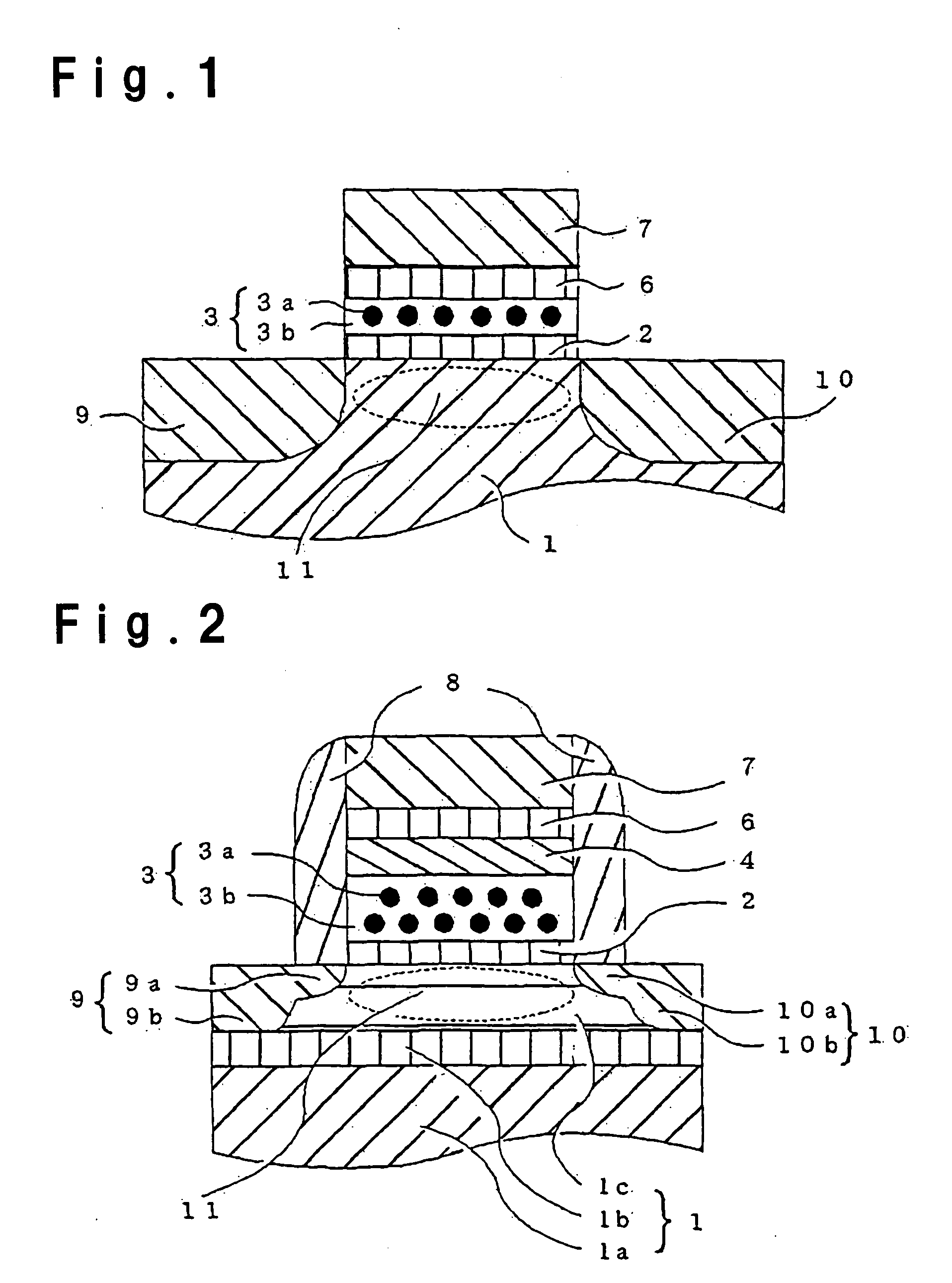
[0079] The nonvolatile semiconductor memory device in this example will be explained, referring to FIG. 1. A tunnel insulating film 2 was formed on a p-type single-crystal Si substrate 1. The tunnel insulating film 2 was prepared by subjecting a semiconductor substrate to thermal oxidation at 800° C. and had a thickness of 3 nm.

[0080] Then, a charge retention layer 3, which was constituted from an insulating matrix 3b containing nano-particles 3a for charge retention, was formed so as to have a thickness of 7 nm by a capacitively coupled type magnetron sputtering method as described below. Metal Co and SiO2 were selected for the nano-particles and the insulating matrix, respectively. When sputtering, a composite target which comprised a metal Co target having a diameter of 6 inches (15.24 cm) and SiO2 glass chips having 5 mm square and placed thereon was employed. The amount of the SiO2 glass chip was adjusted to occupy 70% of the area of the surface that was exposed to plasma of t...

example 2

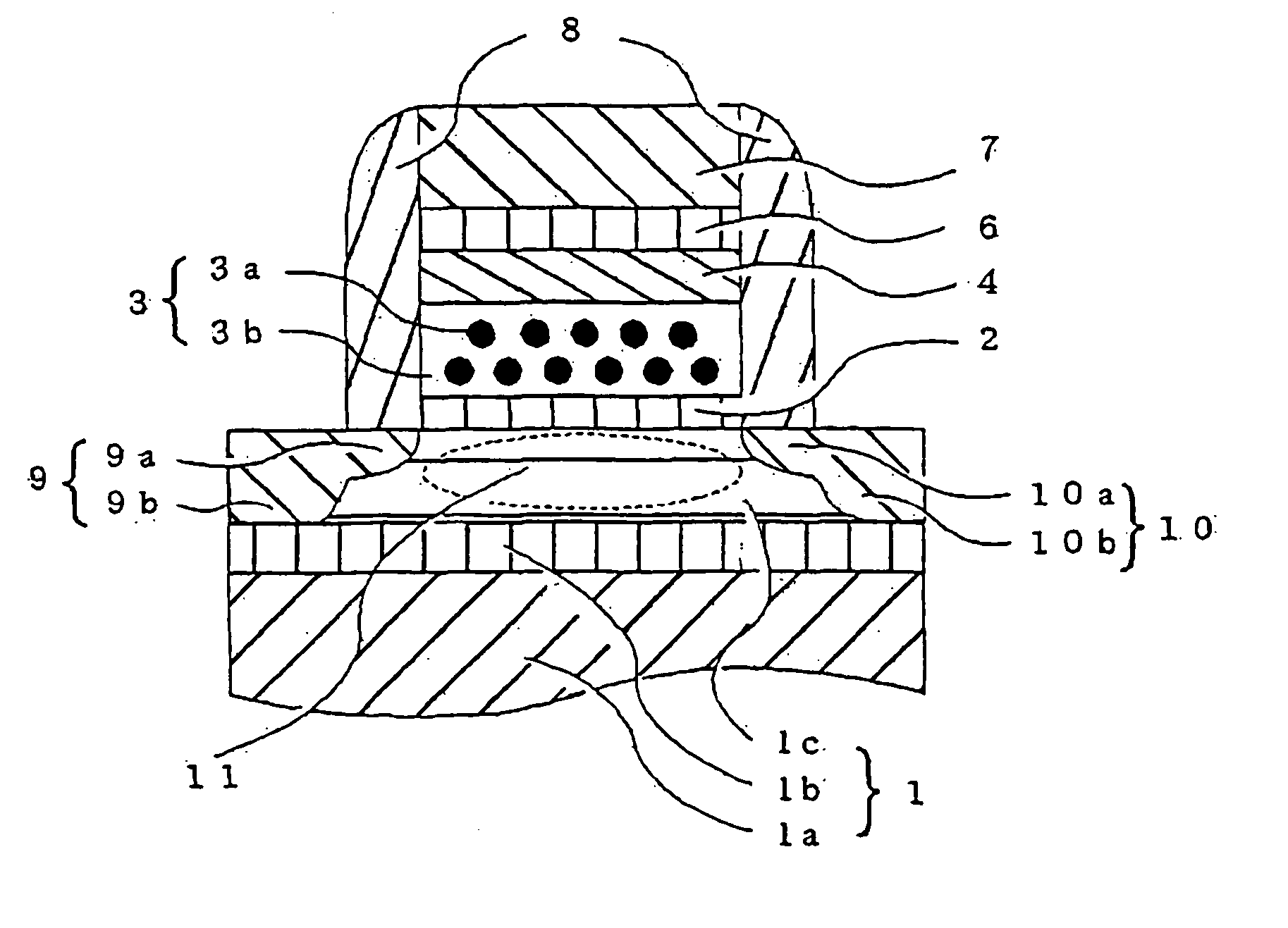
[0084] The nonvolatile semiconductor memory device in this example will be explained, referring to FIG. 2. By a mesa separation method, each device cell on an SOI substrate was isolated, the SOI substrate comprised a p-type single-crystal Si substrate 1a, a buried oxide film 1b and a p-type SOI layer 1c. An oxide film as a tunnel insulating film 2 was formed on the p-type SOI layer 1c so as to have a thickness of 1.5 nm by thermal oxidation at 800° C.

[0085] And then, a charge retention layer 3 which comprised an insulating matrix 3b three-dimensionally containing nano-particles 3a was formed so as to have a thickness of 10 nm by a sputtering method in the manner described below. A thin film comprising two-phases of Pt and SiO2 was formed. When sputtering, a composite target with a diameter of 6 inches (15.24 cm) which was prepared by mixing Pt powder and SiO2 powder with a volume proportion of 20:80 and then sintering the mixture was employed.

[0086] After evacuating the film depos...


PUM

PropertyMeasurementUnit
Particle sizeaaaaaaaaaa
Nanoscale particle sizeaaaaaaaaaa
Particle diameteraaaaaaaaaa

Abstract

There is provided a nonvolatile semiconductor memory device which can shorten data writing and erasing time, significantly improve the endurance characteristic and be activated with low power consumption. The nonvolatile semiconductor memory device comprises an insulating layer 3b with electric insulation, wherein, a charge retention layer 3 formed adjacent to a tunnel insulating film 2 contains nano-particles 3a comprised of a compound which is constituted from at least one single-element substance or chemical compound having a particle diameter of at most 5 nm functions as a floating gate, and which are independently dispersed with a density of from 10+12 to 10+14 particles per square centimeter.

Description

TECHNICAL FIELD [0001] The present invention relates to a nonvolatile semiconductor memory device and a process for manufacturing the same, specifically, a nonvolatile semiconductor memory device which has a structure constituted from an insulating matrix having nano-particles that are comprised of at least one type of single-element substance or at least one type of chemical compound and are dispersed with high density, and which has a charge retention layer having an excellent retention ability, and a process for manufacturing the device at a low cost and with good reproducibility. BACKGROUND ART [0002] Conventionally, as recording media that can record and rewrite a large volume of data, memory devices employing a semiconductor, such as DRAMs or SRAMs, and rotating disk type recording media, such as hard disks, magnetic optical disks or an optical disks, have been available. Systems employing any one of the recording media have been developed and used. Among these recording media...

Claims


Application Information

Patent Timeline
IPC IPC(8): C23C14/06H01L21/28H01L21/336H01L21/8247H01L27/115H01L29/423H01L29/788H01L29/792
CPCB82Y10/00H01L21/28273H01L21/28282H01L29/42332H01L29/42348Y10S977/936H01L29/66833H01L29/7883H01L29/7888Y10S977/773H01L29/66825H01L29/40114H01L29/40117
Inventor KOYANAGI, MITSUMASATAKATA, MASAAKIKONDOH, SHINJI
Owner ASAHI GLASS CO LTD
Learn More