Aluminum/ceramic bonding substrate and method for producing same

a technology of aluminum/ceramic bonding and substrate, which is applied in the direction of natural mineral layered products, metallic pattern materials, solid-state devices, etc., can solve the problems of difficult control of aluminum grain size, increased grain size, and increased production cost, so as to reduce the variation in grain size distribution, prevent cracks, and reduce the effect of aluminum grain siz

Active Publication Date: 2005-04-07
DOWA METALTECH CO LTD
View PDF8 Cites 11 Cited by
  • Summary
  • Abstract
  • Description
  • Claims
  • Application Information

AI Technical Summary

Benefits of technology

[0012] It is therefore an object of the present invention to eliminate the aforementioned problems and to provide an aluminum / ceramic bonding substrate capable of decreasing the grain size of aluminum to decrease the variation in grain size distribution to prevent cracks from being produced in a ceramic substrate after heat cycles, and of controlling the warpage of an aluminum base plate due to heat when a semiconductor chip or the like is soldered thereon, to inhibit the heat sink characteristic of the aluminum base plate from deteriorating when a radiating fin or the like is mounted thereon, and a method for producing the same.
[0014] It is another object of the present invention to provide an aluminum / ceramic bonding substrate having good insulating characteristics by decreasing the grain size of an aluminum-silicon alloy of an aluminum alloy member, which is bonded to a ceramic substrate, to prevent the macroscopic segregation of silicon to prevent silicon from remaining on the surface of the ceramic substrate, and a method for producing same. It is a further object of the present invention to provide an aluminum / ceramic bonding substrate capable of preventing solder cracks from being produced by heat cycles and of preventing the heat sink characteristic of the substrate from deteriorating, even if a heat sink plate is soldered thereon, and a method for producing the same.
[0016] According to one aspect of the present invention, there is provided a method for producing an aluminum / ceramic bonding substrate wherein an aluminum member is bonded directly to a ceramic substrate, the method comprising the steps of: preparing an additive for decreasing a grain size of an aluminum member to 10 mm or less while preventing a drop in thermal conductivity of the aluminum member from a thermal conductivity of a member of pure aluminum from exceeding 20% of the thermal conductivity of the member of pure aluminum; arranging a ceramic substrate in a mold; adding the additive to molten aluminum which is injected into the mold so as to contact one side of the ceramic substrate; and cooling the mold to solidify the molten aluminum to form an aluminum member on the one side of the ceramic substrate so that the aluminum member is bonded directly to the one side of the ceramic substrate.

Problems solved by technology

Therefore, if the base plate warps during soldering, when the radiating fin or cooling jacket is mounted on the base plate, the clearance therebetween increases, so that there is a problem in that the heat sink characteristic of the base plate extremely deteriorates.
However, in the molten metal bonding method, it is difficult to control the grain size of aluminum, so that the obtained grain size of aluminum is a large grain size of 10 mm or more.
Thus, cracks are easily produced in the ceramic substrate after heat cycles, and the behavior of warpage of the aluminum base plate varies due to heat when semiconductor chips are soldered thereon.
However, in a conventional aluminum / ceramic bonding substrate, if an aluminum member is plated with nickel or the like to bond thereon a heat sink plate, such as a copper plate, via solder, there are some cases where cracks are produced in the solder by heat cycles, so that the heat sink characteristic of the heat sinkplate deteriorates.
It is considered that such solder cracks are produced in the relatively weak solder layer by stress which is produced on the bonding interface by heat cycles due to the difference in coefficient of thermal expansion between the aluminum member and the solder.
However, when an aluminum alloy member of an aluminum-silicon alloy, particularly an aluminum alloy containing 0.1 to 1.5 wt % of silicon, is bonded to a ceramic substrate by the molten metal bonding method, if the current cooling method is used, it is very difficult to decrease the grain size of the alloy by optimizing usual cooling conditions, and it is very difficult to control the formation of a solid solution of silicon in aluminum.
Thus, there is a problem in that the enriching section of silicon exists in the aluminum alloy member.
Thus, there are some cases where hot cracks are produced in the aluminum alloy member during the cooling process, so that the aluminum / ceramic bonding substrate does not function as a normal aluminum / ceramic bonding substrate.
In addition, if etching is carried out for forming a circuit on the aluminum alloy member, there are some cases where the enriching section of silicon remains on the surface of the ceramic substrate without being dissolved, so that it is not possible to obtain the desired insulating characteristics of the aluminum / ceramic bonding substrate.

Method used


Image

  • Aluminum/ceramic bonding substrate and method for producing same
  • Aluminum/ceramic bonding substrate and method for producing same
  • Aluminum/ceramic bonding substrate and method for producing same

Examples


example 1

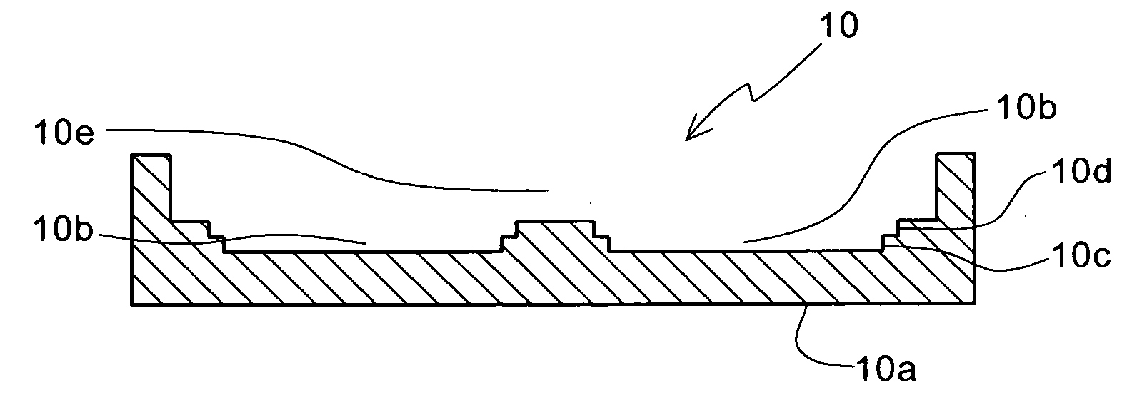
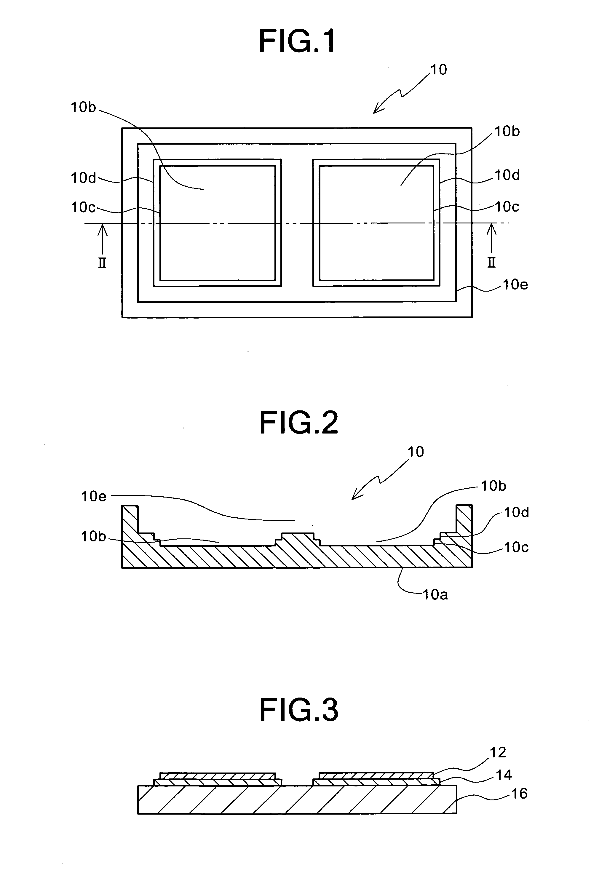
[0042] First, as shown in FIGS. 1 and 2, a carbon mold having a lower mold member 10 was prepared as a mold. The lower mold member 10 has a bottom portion 10a having a substantially rectangular planar shape. The top surface of the bottom portion 10a of the lower mold member 10 has two recessed portions 10b which are spaced from each others by 10 mm and each of which has a step-wise extending side wall. Each of the recessed portions 10b comprises: an aluminum plate forming portion 10c capable of forming an aluminum plate having a size of 39 mm×39 mm×0.4 mm; and a ceramic substrate housing portion 10d which is formed above the aluminum plate forming portion 10c so as to be adjacent thereto and which substantially has the same shape and size as those of a ceramic substrate having a size of 40 mm×40 mm×0.635 mm so as to be capable of housing therein the ceramic substrate. When an upper mold member (not shown) having a substantially rectangular planar shape is put on the lower mold membe...

example 2

[0050] With respect to a bonding article obtained by the same method as that in Example 1, except that the same Al—Ti—B alloy as that in Example 1 was added so that the content of Ti was 0.1 wt %, the same evaluation as that in Example 1 was carried out. As a result, the grain size of aluminum on the reverse of the aluminum base plate was in the range of from about 3 mm to about 5 mm. In addition, no bonding failure was detected on the bonding interface between the aluminum circuit plate and the ceramic substrate and on the bonding interface between the ceramic substrate and the aluminum base plate, and no crack was observed on the ceramic substrate. In addition, the variation in warpage before and after heating was so small as to be in the range of −20 μm to 30 μm. Also after heat cycles were repeatedly carried out three thousands times, no bonding failure was detected, and no crack was observed on the ceramic substrate. Moreover, the thermal conductivity of a sample cut out of the...

example 3

[0051] With respect to a bonding article obtained by the same method as that in Example 1, except that calcium (Ca) was added in place of the Al—Ti—B alloy, the same evaluation as that in Example 1 was carried out. As a result, the grain size of aluminum on the reverse of the aluminum base plate was in the range of from about 5 mm to about 10 mm. In addition, no bonding failure was detected on the bonding interface between the aluminum circuit plate and the ceramic substrate and on the bonding interface between the ceramic substrate and the aluminum base plate, and no crack was observed on the ceramic substrate. In addition, the variation in warpage before and after heating was in the range of −50 μm to 50 μm and was not so great. Also after heat cycles were repeatedly carried out three thousands times, no bonding failure was detected, and no crack was observed on the ceramic substrate. Moreover, the thermal conductivity of a sample cut out of the obtained bonding article was 214 W / ...


PUM

PropertyMeasurementUnit
grain sizeaaaaaaaaaa
thicknessaaaaaaaaaa

Abstract

When an aluminum plate is bonded directly to a ceramic substrate by cooling and solidifying molten aluminum which is injected into a mold so as to contact the ceramic substrate arranged in the mold, an additive, such as a TiB alloy, Ca or Sr, for decreasing the grain size of the aluminum plate to 10 mm or less while preventing the drop in thermal conductivity of the aluminum plate from the thermal conductivity of a pure aluminum plate from exceeding 20% of the thermal conductivity of the pure aluminum plate is added to the molten aluminum. When an aluminum alloy plate of an aluminum-silicon alloy is bonded directly to a ceramic substrate by cooling and solidifying a molten aluminum-silicon alloy which is injected into a mold so as to contact the ceramic substrate arranged in the mold, an aluminum-silicon alloy containing 0.1 to 1.5 wt % of silicon and 0.03 to 0.10 wt % of boron is injected into the mold.

Description

BACKGROUND OF THE INVENTION [0001] 1. Field of the Invention [0002] The present invention generally relates to an aluminum / ceramic bonding substrate and a method for producing the same. More specifically, the invention relates to an aluminum / ceramic bonding substrate wherein an aluminum member is bonded to at least one side of a ceramic substrate, and a method for producing the same. [0003] 2. Description of the Prior Art [0004] In recent years, power modules are used for controlling heavy-current for electric vehicles, electric railcars, machine tools and so forth. In a conventional power module, a metal / ceramic insulating substrate is fixed to one side of a metal plate or compound material called base plate by soldering, and one or a plurality of semiconductor chips are fixed to the metal / ceramic insulating substrate by soldering. On the other side (reverse) of the base plate, a radiating fin or cooling jacket of a metal is mounted via a thermal conduction grease by means of screw...

Claims


Application Information

Patent Timeline
Patent Type & Authority Applications(United States)
IPC IPC(8): C04B37/02C04B41/51C04B41/52C04B41/88C04B41/89C04B41/90H01L23/373H05K1/09H05K3/10
CPCB32B2311/24Y10T428/12736C04B41/009C04B41/5155C04B41/52C04B41/88C04B41/89C04B41/90C04B2111/00844C04B2235/6584C04B2235/96C04B2235/9607C04B2235/963C04B2237/402H01L23/3735H05K1/09H05K3/101H05K2203/128C04B37/021Y10T428/1275Y10T428/12611Y10T428/12007Y10T428/12535H01L2924/0002C04B41/4523C04B41/5094C04B41/5096C04B41/4541C04B41/5144C04B35/10C04B35/581H01L2924/00Y10T428/31678
Inventor OSANAI, HIDEYOIDEGUCHI, SATORU
Owner DOWA METALTECH CO LTD
Why Eureka
Try Eureka