Organic field effect transistor semiconductor layer P-type doping method and prepared organic field effect transistor
A technology of organic semiconductor layers and transistors, which is applied in semiconductor/solid-state device manufacturing, semiconductor devices, electric solid-state devices, etc., and can solve problems such as on-off ratio attenuation and performance degradation.
- Summary
- Abstract
- Description
- Claims
- Application Information
AI Technical Summary
Problems solved by technology
Method used
Image

Examples
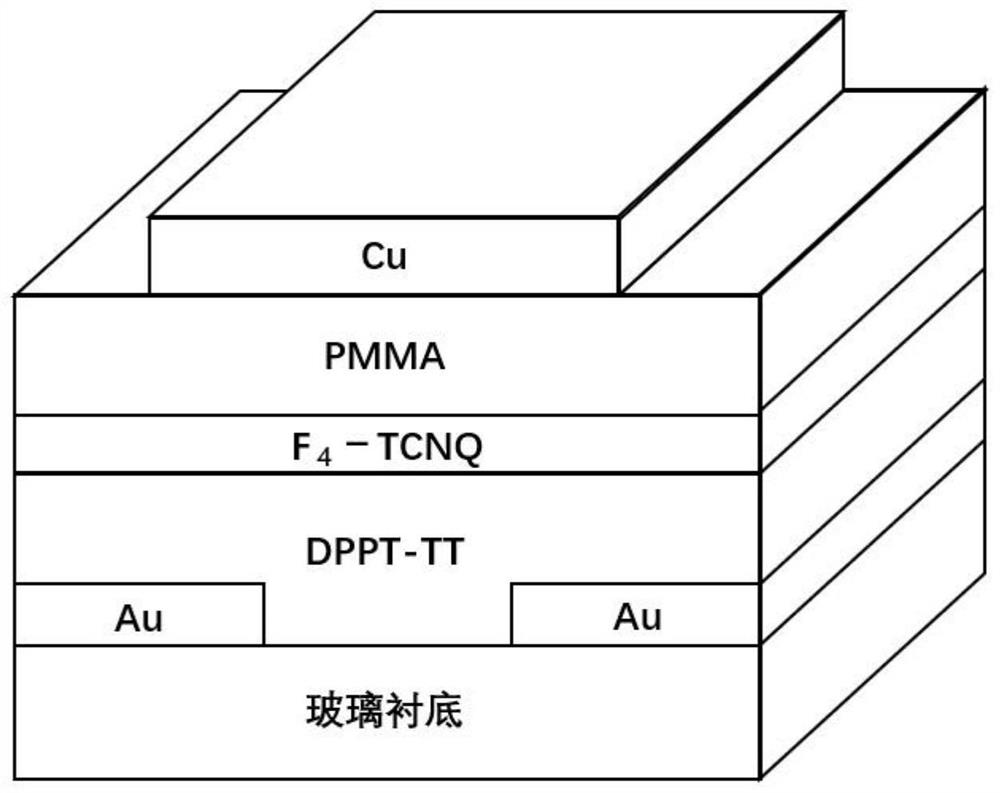
Embodiment 1
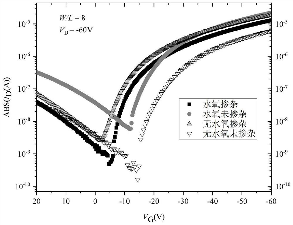
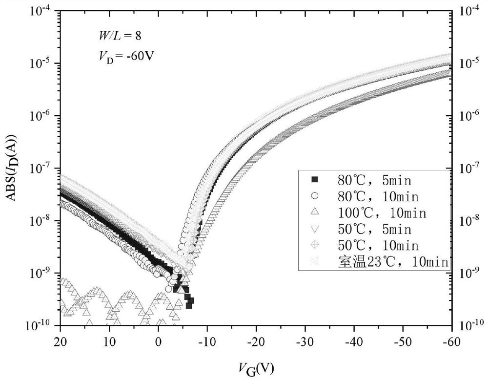
[0034] Example 1 Doping under the condition of water and oxygen atmosphere
[0035] The present embodiment relates to a process including P-type channel doping by a solution method in a water-oxygen atmosphere and a method for fabricating a polymer field effect transistor, which specifically includes the following specific steps:
[0036] 1) Substrate cleaning: a glass sheet is used as the substrate. Put the glass pieces into beakers of deionized water (DI) and ethanol respectively, use an ultrasonic cleaning machine to clean them for 5-10 minutes, repeat the operation 2 times, and then use high-purity nitrogen (purity 99.99%) to clean the glass pieces. The surface was blown dry, and the glass sheet was thoroughly dried by heating at 100 °C for 20 minutes on a heating table, and used as a substrate;
[0037] 2) Surface treatment: Clean the dried glass sheets with an ultraviolet ozone cleaning machine (U / V ozone) for 30 minutes to remove organic residues on the surface of the ...
PUM
| Property | Measurement | Unit |
|---|---|---|
| Thickness | aaaaa | aaaaa |
| Thickness | aaaaa | aaaaa |
Abstract
Description
Claims
Application Information
 - R&D
- Intellectual Property
- Life Sciences
- Materials
- Tech Scout
- Unparalleled Data Quality
- Higher Quality Content
- 60% Fewer Hallucinations
Browse by: Latest US Patents, China's latest patents, Technical Efficacy Thesaurus, Application Domain, Technology Topic, Popular Technical Reports.
© 2025 PatSnap. All rights reserved.Legal|Privacy policy|Modern Slavery Act Transparency Statement|Sitemap|About US| Contact US: help@patsnap.com