A preparation method of high thermal conductivity diamond-reinforced silicon carbide substrate
A diamond-enhanced, silicon carbide substrate technology, applied in semiconductor/solid-state device manufacturing, electrical components, circuits, etc., can solve the interface strength between SiC and diamond, thermal conductivity of nucleation defects, etching interface strength, interface thermal stress, etc. question
- Summary
- Abstract
- Description
- Claims
- Application Information
AI Technical Summary
Problems solved by technology
Method used
Image
Examples
specific Embodiment approach 1
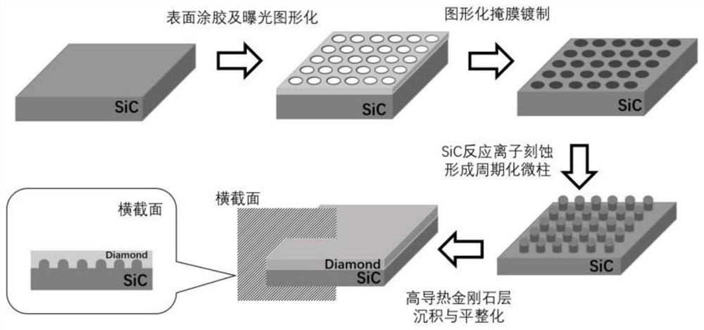
[0030] UV lithography is achieved by spin-coating photoresist on the carbon polar side of SiC and through a mask-based mask. Then, periodic micropores with a diameter of 2 μm and an interval of 4 μm are realized by developing and degumming, and the periodically arranged diamond patterned surface is exposed. The SiC with patterned photoresist was first deposited with a Ti metal mask of 50 nm and then deposited with an Al metal of 150 nm by electron beam evaporation. Then, after removing the residual photoresist, SiC with a metal pattern mask deposited on the surface is obtained. on SiC by taking the gas source CF 4 :O 2 The SiC was etched to an etching depth of 2 μm under the condition of a ratio of 5:1 and a bias power of 300 W. The metal mask is then removed by chemical dissolution. The SiC is then passed through pure CF again 4 The SiC was etched under the bias power of 20W to realize the arc-shaped etching of the edge of the micropillar. Then, the patterned SiC sheet ...
specific Embodiment approach 2
[0031] UV lithography is achieved by spin-coating photoresist on the carbon polar side of SiC and through a mask-based mask. Then, periodic micropores with a diameter of 2 μm and an interval of 2 μm are realized by developing and degumming, and the periodically arranged diamond patterned surface is exposed. The SiC with patterned photoresist was first deposited with a Ti metal mask of 30 nm and then deposited with an Al metal of 120 nm by electron beam evaporation. Then, after removing the residual photoresist, SiC with a metal pattern mask deposited on the surface is obtained. on SiC by taking the gas source CF 4 :O 2 The SiC was etched to an etching depth of 1 μm under the condition of a ratio of 4:1 and a bias power of 200 W. The metal mask is then removed by chemical dissolution. The SiC is then passed through pure CF again 4 The SiC was etched under the bias power of 10W to realize the arc-shaped etching of the edge of the micropillar. Then, the patterned SiC sheet ...
specific Embodiment approach 3
[0032] UV lithography is achieved by spin-coating photoresist on the carbon polar side of SiC and through a mask-based mask. Then, periodic micropores with a diameter of 5 μm and an interval of 8 μm are realized by developing and degumming, and the periodically arranged diamond patterned surface is exposed. The SiC with patterned photoresist was first deposited with a Ti metal mask of 40 nm and then deposited with an Al metal of 150 nm by electron beam evaporation. Then, after removing the residual photoresist, SiC with a metal pattern mask deposited on the surface is obtained. on SiC by taking the gas source CF 4 :O 2 The SiC was etched to an etching depth of 3 μm under the condition of a ratio of 2:1 and a bias power of 100 W. The metal mask is then removed by chemical dissolution. The SiC is then passed through pure CF again 4 The SiC was etched under the bias power of 10W to realize the arc-shaped etching of the edge of the micropillar. Then, the patterned SiC sheet ...
PUM
| Property | Measurement | Unit |
|---|---|---|
| thermal conductivity | aaaaa | aaaaa |
| electrical resistivity | aaaaa | aaaaa |
Abstract
Description
Claims
Application Information
 - R&D
- Intellectual Property
- Life Sciences
- Materials
- Tech Scout
- Unparalleled Data Quality
- Higher Quality Content
- 60% Fewer Hallucinations
Browse by: Latest US Patents, China's latest patents, Technical Efficacy Thesaurus, Application Domain, Technology Topic, Popular Technical Reports.
© 2025 PatSnap. All rights reserved.Legal|Privacy policy|Modern Slavery Act Transparency Statement|Sitemap|About US| Contact US: help@patsnap.com

