N surface yellow-light LED material based on c-surface sapphire substrate and manufacturing method thereof
A sapphire substrate, yellow light technology, applied in the field of microelectronics, can solve the problems of complex quantum well growth process, degraded GaN crystal quality, affecting device performance, etc., to improve growth efficiency, avoid large lattice mismatch of materials, and simplify The effect of the process steps
- Summary
- Abstract
- Description
- Claims
- Application Information
AI Technical Summary
Problems solved by technology
Method used
Image

Examples
Embodiment 1
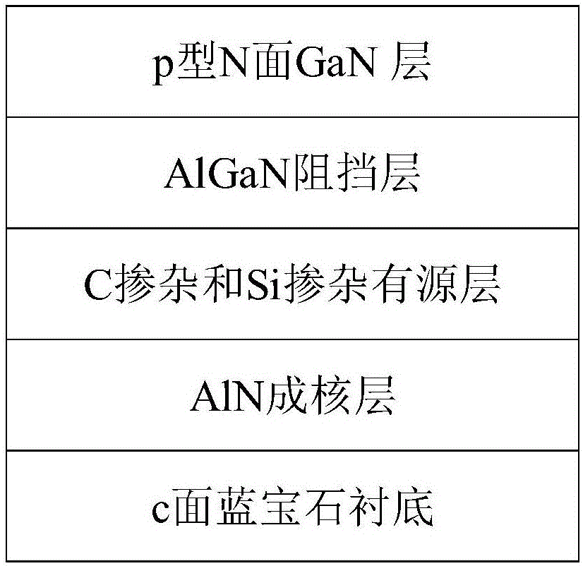
[0026] Embodiment 1, making the C doping concentration is 1×10 18 cm -3 , Si doping concentration is 2×10 18 cm -3 The n-type N-face GaN active layer LED material.
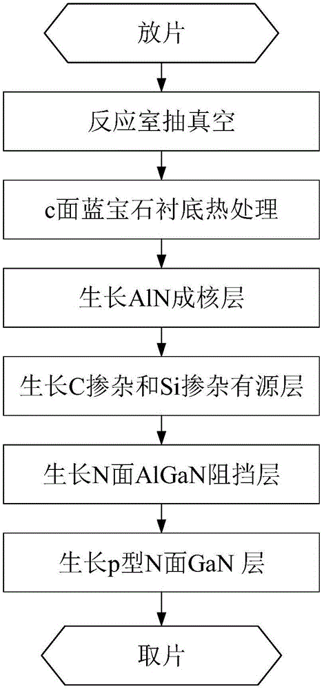
[0027] Step 1, performing heat treatment on the substrate substrate.
[0028] Place the c-plane sapphire substrate in the metal organic chemical vapor deposition MOCVD reaction chamber, and pass the mixed gas of hydrogen and ammonia into the reaction chamber, and the vacuum degree in the reaction chamber is less than 2×10 -2 Torr, under the conditions that the substrate heating temperature is 1050° C., the time is 8 minutes, and the pressure of the reaction chamber is 35 Torr, heat treatment is performed on the substrate.
[0029] Step 2, growing an AlN nucleation layer.
[0030] Lower the temperature of the heat-treated substrate to 580°C, feed the aluminum source with a flow rate of 4 μmol / min, hydrogen gas with a flow rate of 1200 sccm and ammonia gas with a flow rate of 5000 sccm, and grow the thickness u...
Embodiment 2
[0037] Embodiment 2, making C doping concentration is 1×10 17 cm -3 , Si doping concentration is 5×10 17 cm -3 The n-type N-face GaN active layer LED material.
[0038] The implementation steps of this example are as follows:
[0039] In step A, the c-plane sapphire substrate is placed in a metal organic chemical vapor deposition MOCVD reaction chamber, and a mixed gas of hydrogen and ammonia is introduced into the reaction chamber, and the vacuum degree in the reaction chamber is less than 2×10 -2Torr, under the condition that the substrate heating temperature is 850° C., the time is 5 minutes, and the reaction chamber pressure is 20 Torr, heat treatment is performed on the substrate.
[0040] Step B, lowering the temperature of the heat-treated substrate to 480°C, feeding an aluminum source with a flow rate of 3 μmol / min, hydrogen gas with a flow rate of 1000 sccm and ammonia gas with a flow rate of 8000 sccm into the reaction chamber, under the condition of maintaining ...
Embodiment 3
[0044] Embodiment 3, making the C doping concentration is 4×10 19 cm -3 , Si doping concentration is 5×10 19 cm -3 The n-type N-face GaN active layer LED material.
[0045] The implementation steps of this example are as follows:
[0046] Step 1: performing heat treatment on the base substrate.
[0047] The c-plane sapphire substrate is placed in a metal organic chemical vapor deposition MOCVD reaction chamber, and a mixed gas of hydrogen and ammonia is introduced into the reaction chamber for heat treatment. The process conditions of heat treatment are as follows:
[0048] The vacuum degree of the reaction chamber: less than 2×10 -2 Torr;
[0049] Substrate heating temperature: 1170°C;
[0050] Nitriding time: 30min;
[0051] Reaction chamber pressure: 750 Torr.
[0052] Step 2, growing an AlN nucleation layer.
[0053] A low-temperature AlN nucleation layer with a thickness of 200 nm is grown on the heat-treated substrate. The process conditions are as follows: ...
PUM
| Property | Measurement | Unit |
|---|---|---|
| Thickness | aaaaa | aaaaa |
| Thickness | aaaaa | aaaaa |
| Thickness | aaaaa | aaaaa |
Abstract
Description
Claims
Application Information
 - Generate Ideas
- Intellectual Property
- Life Sciences
- Materials
- Tech Scout
- Unparalleled Data Quality
- Higher Quality Content
- 60% Fewer Hallucinations
Browse by: Latest US Patents, China's latest patents, Technical Efficacy Thesaurus, Application Domain, Technology Topic, Popular Technical Reports.
© 2025 PatSnap. All rights reserved.Legal|Privacy policy|Modern Slavery Act Transparency Statement|Sitemap|About US| Contact US: help@patsnap.com