
Patsnap Eureka
For R&D, Patsnap Eureka makes reading and utilizing patents & technical documents easy.
Patsnap Eureka AIR
Designed for self-driven R&D workflows. Generate viable solutions, solve complex R&D challenges, empower your innovation with AI.

Patsnap Eureka Materials
Designed for material experts only. Revolutionize your material R&D, from search, analyze, to developing new materials.

TechResearch
Generate reliable direction feasibility study reports for your R&D in just a few steps.

TechSeek
Discover and master advanced knowledge NOW. Basics, ideas, possibilities, all at once.

TechMind
As an expert in R&D Theories, TechMind can generates customized viable solutions instantly.

TechRisk
Analyze your overall solution with one click, know your potential R&D risks in advance.

TechMonitor
Get weekly tech updates, stay abreast of the latest tech innovations and key insights.
A kind of gan-based vertical cavity surface emitting laser and its preparation method
A vertical cavity surface emission and laser technology, applied in lasers, laser parts, semiconductor lasers, etc., can solve the problems affecting device performance, poor sapphire electrical conductivity, poor thermal conductivity, etc., achieving a simple preparation method, improving yield and device performance. , the effect of reducing costs
- Summary
- Abstract
- Description
- Claims
- Application Information
AI Technical Summary
Problems solved by technology
Method used
Image

Examples
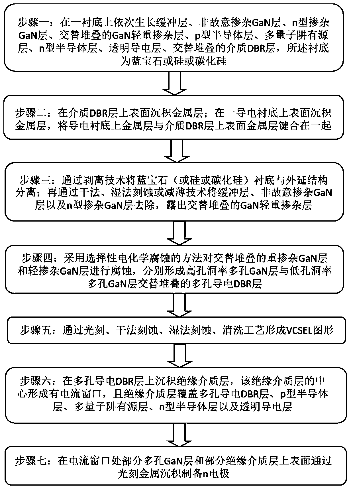
Embodiment 1
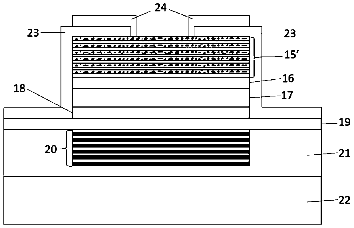
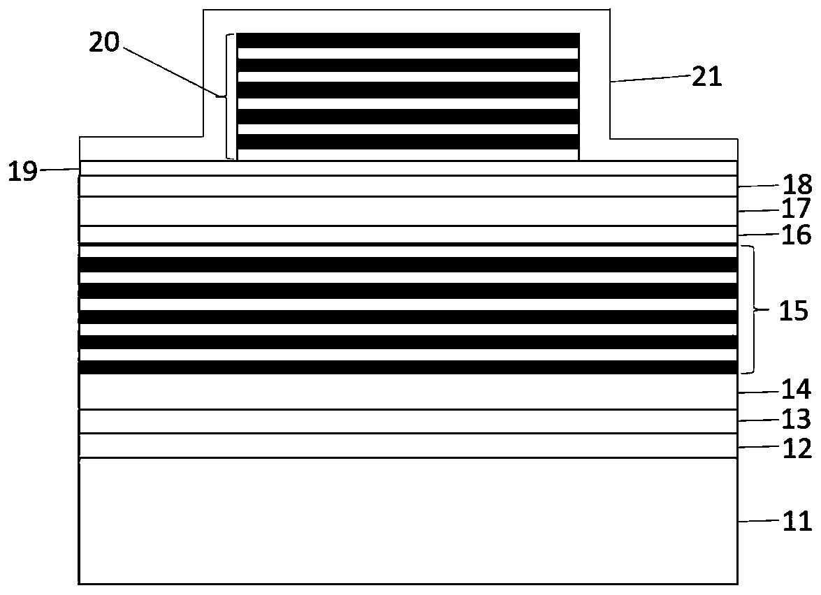
[0046] A GaN-based vertical cavity surface emitting laser, such as figure 1 As shown, a conductive substrate 22 is included. A metal layer 21 is formed on the upper surface of the conductive substrate 22. A window is arranged in the middle of the upper surface of the metal layer 21. A dielectric DBR layer 20 is made at the window in the middle part of the upper surface of the metal layer 21. The dielectric DBR Layer 20 upper surface is made with transparent conductive layer 19, transparent conductive layer 19 covers medium DBR layer 20 and metal layer 21; The semiconductor layer 16, the upper surface of the n-type semiconductor layer 16 is grown to prepare a porous conductive DBR layer 15', the upper surface of the porous conductive DBR layer 15' is made with an insulating medium layer 23, and the middle of the insulating medium 23 layer forms a current window, and the insulating medium layer 23 covers the porous conductive DBR layer 15', the n-type semiconductor layer 16, the...
Embodiment 2
[0048] A GaN-based vertical cavity surface-emitting laser, the structure of which is shown in Embodiment 1, the difference is that the porous conductive DBR layer 15' is a multi-period DBR formed by alternately stacking high-porosity porous GaN layers and low-porosity porous GaN layers structure, the high-porosity porous GaN layer and the low-porosity porous GaN layer are formed by electrochemical corrosion of the heavily doped GaN layer and the lightly doped GaN layer respectively, and the dopants of the lightly doped GaN layer and the heavily doped GaN layer is silicon, and its doping concentration is 5×10 17 cm -3 and 5×10 19 cm -3 .
Embodiment 3
[0050] A GaN-based vertical cavity surface emitting laser, the structure is as shown in embodiment 1, the difference is, as figure 1 As shown, the period number of the porous conductive DBR layer 15' of this embodiment is 6, the reflectivity is less than 99.8%, and the aperture of the porous conductive DBR layer 15' is 1-300nm.
PUM
| Property | Measurement | Unit |
|---|---|---|
| pore size | aaaaa | aaaaa |
| thickness | aaaaa | aaaaa |
| reflectance | aaaaa | aaaaa |
Abstract
Description
Claims
Application Information
 - R&D Engineer
- R&D Manager
- IP Professional
- Industry Leading Data Capabilities
- Powerful AI technology
- Patent DNA Extraction
Browse by: Latest US Patents, China's latest patents, Technical Efficacy Thesaurus, Application Domain, Technology Topic, Popular Technical Reports.
© 2024 PatSnap. All rights reserved.Legal|Privacy policy|Modern Slavery Act Transparency Statement|Sitemap|About US| Contact US: help@patsnap.com