Electrolyte gate oxide semiconductor phototransistor for ultraviolet light detection
An oxide semiconductor and phototransistor technology, applied in semiconductor devices, circuits, electrical components, etc., can solve problems such as reducing the UV-Vis rejection ratio, and achieve increased UV-Vis rejection ratio, improved stability, and fast light response speed. Effect
- Summary
- Abstract
- Description
- Claims
- Application Information
AI Technical Summary
Problems solved by technology
Method used
Image
Examples
Embodiment 1
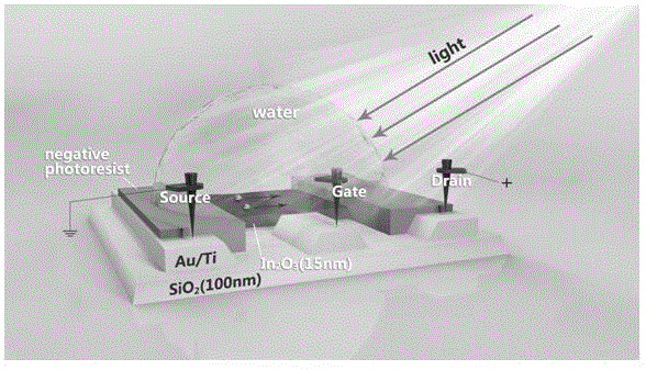
[0030] figure 1 It is a schematic diagram of the structure of the indium oxide thin film transistor ultraviolet light detector in the first embodiment of the present invention. Regarding the specific symbols in the figure, 1 represents a quartz substrate, 2, 3, and 4 represent titanium source, drain, and gate electrodes, respectively, 5 represents an indium oxide active layer, 6 represents a negative glue protective layer, and 7 represents an electrolyte.
[0031] The thin film transistor in the first embodiment can be manufactured as follows:
[0032] 1) Put the quartz substrate into the MOCVD epitaxy equipment to grow 15nm indium oxide film. The specific growth conditions are as follows: use trimethylindium as the indium source and oxygen as the oxygen source, the epitaxial growth temperature is 421℃, and under an argon atmosphere The pressure in the reaction chamber is controlled to 7.1 Torr, and the flow rate of trimethyl indium is 3×10 -5 Mol / min, the flow rate of oxygen is co...
PUM
 Abstract
Description
Claims
Application Information
 - R&D
- Intellectual Property
- Life Sciences
- Materials
- Tech Scout
- Unparalleled Data Quality
- Higher Quality Content
- 60% Fewer Hallucinations
Browse by: Latest US Patents, China's latest patents, Technical Efficacy Thesaurus, Application Domain, Technology Topic, Popular Technical Reports.
© 2025 PatSnap. All rights reserved.Legal|Privacy policy|Modern Slavery Act Transparency Statement|Sitemap|About US| Contact US: help@patsnap.com


