Fin-type field-effect tube formation method

A fin field effect tube and fin technology, which is applied in the direction of semiconductor devices, electrical components, circuits, etc., can solve the problems that the electrical performance of the fin field effect tube needs to be improved, so as to avoid the shadow effect, improve the electrical performance, and block the effect weak effect

Active Publication Date: 2017-04-19
SEMICON MFG INT (SHANGHAI) CORP +1
View PDF2 Cites 0 Cited by
  • Summary
  • Abstract
  • Description
  • Claims
  • Application Information

AI Technical Summary

Problems solved by technology

[0005] However, the electrical performance of the fin field effect transistor formed by the prior art needs to be improved

Method used


Image

  • Fin-type field-effect tube formation method
  • Fin-type field-effect tube formation method
  • Fin-type field-effect tube formation method

Examples


Embodiment Construction

[0032] It can be seen from the background art that the electrical performance of the fin field effect transistor formed in the prior art needs to be improved.

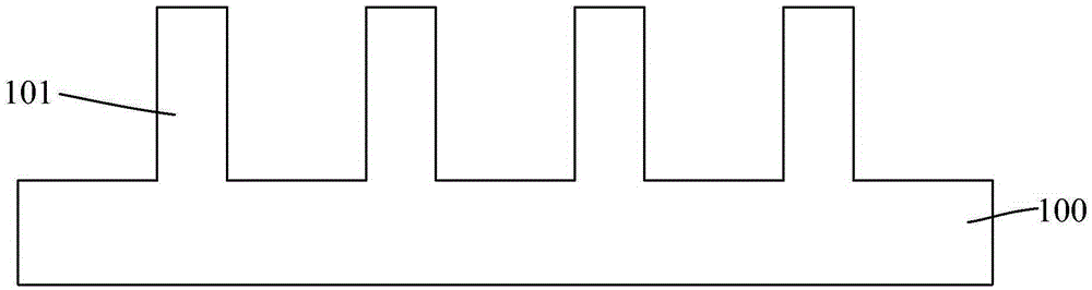
[0033] According to the research on the formation method of FinFET, refer to figure 1 , provide the substrate 100, after forming several discrete fins 101 on the substrate 100, it is usually necessary to perform ion implantation on the fins 101, and doping the fins 101 to improve the electrical performance of the fin field effect transistor, such as the threshold voltage ( Vt), saturation current (Idsat), etc.

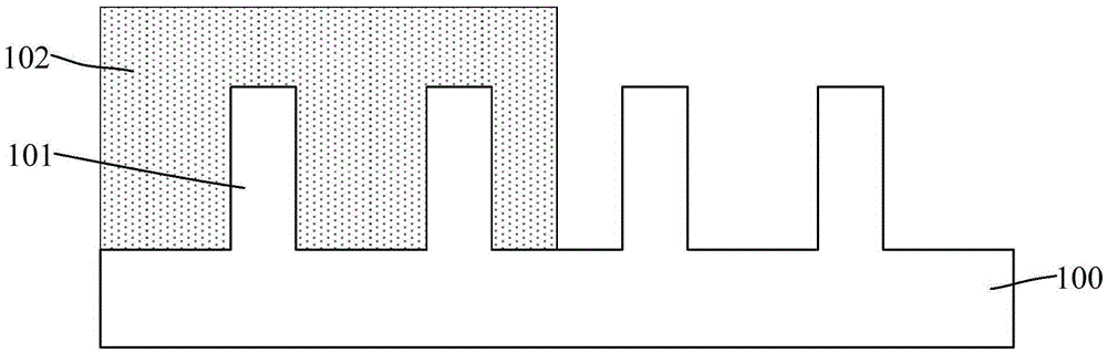
[0034] The process steps of doping the fin portion 101 include: figure 2 , forming an initial photoresist layer covering the substrate 100 and the surface of the fin portion 101; exposing the initial photoresist layer; using a developer to clean the exposed initial photoresist layer to form a patterned photoresist layer The resist layer 102 exposes part of the surface of the fin portion 101 and the substrat...


PUM


Abstract

Provided is a fin-type field-effect tube formation method, which comprises the following steps: providing a substrate, wherein a plurality of separated fins are formed on the surface of the substrate; forming an initial hard mask on the top and side surfaces of the fins and the surface of the substrate; patterning the initial hard mask to form a hard mask layer, wherein the hard mask layer exposes a part of the top and side surfaces of the fins; with the hard mask layer being as a mask, carrying out ion implantation on the exposed fins; and removing the hard mask layer. The method improves the problem of shadow effect in the ion implantation technology, and thus electrical performance of a formed fin-type field-effect tube is improved.

Description

technical field [0001] The invention relates to the technical field of semiconductor manufacturing, in particular to a method for forming a fin field effect transistor. Background technique [0002] With the continuous development of semiconductor process technology, the development trend of semiconductor process nodes following Moore's Law continues to decrease. In order to adapt to the reduction of process nodes, the channel length of MOSFET field effect transistors has to be continuously shortened. The shortening of the channel length has the advantages of increasing the die density of the chip and increasing the switching speed of the MOSFET field effect tube. [0003] However, as the channel length of the device is shortened, the distance between the source and the drain of the device is also shortened, so that the control ability of the gate to the channel becomes worse, and the gate voltage pinches off the channel. The difficulty is also increasing, making the pheno...

Claims


Application Information

Patent Timeline
Patent Type & Authority Applications(China)
IPC IPC(8): H01L21/336H01L21/265
CPCH01L29/66795H01L21/265
Inventor 赵海
Owner SEMICON MFG INT (SHANGHAI) CORP
Why Eureka
Try Eureka