
III nitride-based double-heterojunction phototransistor

A phototransistor and double heterojunction technology, which is applied in the field of visible light and ultraviolet light detectors, can solve the problems of reducing carrier transport efficiency and performance stability, not setting an incident window layer and light absorption layer, quantum efficiency and gain. Improvement and other issues, to achieve the effect of increasing photogenerated electron-hole pairs, reducing base potential, and improving light incident efficiency

Inactive Publication Date: 2016-07-06
SUN YAT SEN UNIV
View PDF3 Cites 10 Cited by
  • Summary
  • Abstract
  • Description
  • Claims
  • Application Information

AI Technical Summary

Problems solved by technology

In 1998, in the article HighgainGaN / AlGaNheterojuncitonphototransistor (AppliedPhysicsLetters, Vol.73, No.7), Wei Yang (Honeywell Technology Center) and others in the United States first published a GaN / AlGaN-based ultraviolet (visible light-blind ultraviolet) heterojunction phototransistor. The device adopts the back-incidence method in which the emission area is placed above and the optical signal is incident from the side of the sapphire substrate. The epitaxial structure of the device needs to grow AlN as a buffer layer first, and then grow AlGaN with a wider band gap than GaN as the incident light window layer. The quality of the epitaxial crystal is reduced, and the dark current of the device is higher.
In 2001, Robert Mouillet et al. of Osaka Gas Company reported in the article Photoresponse and defect levels of AlGaN / GaNheterobipolarphototransistorgrownonlow-temperatureAlNinterlayer (Jpn.J.Appl.Phys, Vol.40, pp.L498-L501) that the normal incidence method was adopted and the collector area was placed on top The visible light-blind AlGaN / GaN heterojunction ultraviolet phototransistor, but the device does not have an incident window layer and a light absorbing layer, and uses a combination of base area exposure and 45-degree angle incidence to realize ultraviolet light detection. Not only the device process is complicated, but also Both quantum efficiency and gain need to be improved
Compared with the previously reported structure, this device structure avoids the problem of crystal quality degradation caused by direct epitaxial AlN buffer layer and AlGaN window layer on the sapphire substrate, but the p-type base region doped with impurity Mg Memory effect and Mg diffusion effect lead to Mg atoms not only confined in the base region, but diffuse upward to the emitter region, resulting in acceptor impurity compensation in the n-type emitter region, thereby reducing the carrier transport efficiency and performance stability in the device

Method used


Image

  • III nitride-based double-heterojunction phototransistor
  • III nitride-based double-heterojunction phototransistor

Examples


Embodiment Construction

[0019] The accompanying drawings are for illustrative purposes only, and should not be construed as limitations on this patent; in order to better illustrate this embodiment, certain components in the accompanying drawings will be omitted, enlarged or reduced, and do not represent the size of the actual product; for those skilled in the art It is understandable that some well-known structures and descriptions thereof may be omitted in the drawings. The positional relationship described in the drawings is for illustrative purposes only, and should not be construed as a limitation on this patent. Unless otherwise specified, the materials and processing methods used in the present invention are conventional materials and processing methods in the technical field.

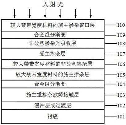
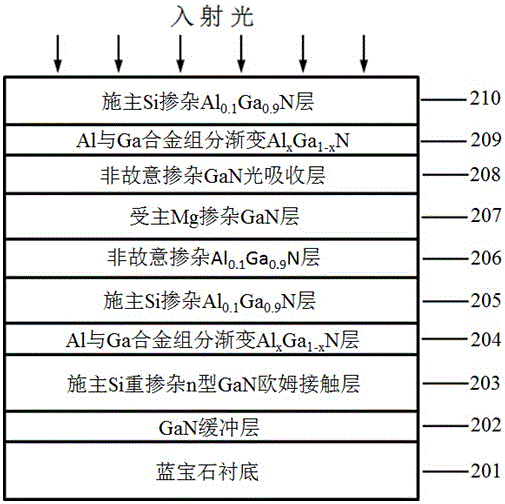
[0020] Such as figure 1 As shown, a Group III nitride-based double heterojunction phototransistor, which includes a substrate 101 and an epitaxial layer grown on the substrate 101, wherein the order of the epitaxial l...


PUM

PropertyMeasurementUnit
thicknessaaaaaaaaaa
thicknessaaaaaaaaaa
thicknessaaaaaaaaaa

Abstract

The invention provides an III nitride-based double-heterojunction phototransistor, belongs to the technical field of semiconductor devices and provides an III nitride-based double-heterojunction phototransistor and a preparation method thereof. The III nitride-based double-heterojunction phototransistor comprises a substrate and an epitaxial layer, wherein the epitaxial layer grows on the substrate; and the epitaxial layer sequentially comprises a buffer layer or a transition layer, a donor heavily-doped ohmic contact layer, an alloy composition gradient layer, a donor doped layer of a relatively broad band gap material, an unintentionally doped layer of the relatively broad band gap material, an acceptor doped layer, an unintentionally doped light absorption layer, the alloy composition gradient layer and a donor heavily-doped window layer of the relatively broad band gap material from bottom to top. By an overhead collector region structure, with the III nitride multi-element alloy material with a relatively broad band gap light absorption layer as the window layer of an incident light, the quantum efficiency is improved; and the number of photo-generated holes is increased, so that the photocurrent gain of the device is improved. A reverse heterojunction is adopted as an emitter junction in a lower emitter region; and the unintentionally doped layer of the relatively broad band gap material is introduced as an acceptor-doped diffusion barrier layer and a base region-emitter region heterointerface energy band sag compensation layer, so that the electron injection efficiency of the transistor is improved. The III nitride-based double-heterojunction phototransistor has the characteristics of high photocurrent gain, stable device performance and the like.

Description

technical field [0001] The present invention relates to the technical field of visible light and ultraviolet light detectors, and more specifically relates to a group III nitride-based double heterojunction phototransistor. Background technique [0002] With the development of information technology, optical detection, optical storage, and optical information detection have higher and higher requirements for detector performance, especially in high-speed, high-frequency, high-temperature applications, which require high gain, low dark current, and high system performance. Noise Ratio Detector. Among photodetectors, p-i-n photodiodes and avalanche photodiodes (APDs) have been widely studied and applied. p-i-n has the characteristics of low working voltage and high quantum efficiency, but has no internal gain and cannot realize weak light detection; APD achieves internal gain through avalanche multiplication, but has high working voltage and large noise. In recent years, pho...

Claims


Application Information

Patent Timeline
Patent Type & Authority Applications(China)
IPC IPC(8): H01L31/11H01L31/0352H01L31/18
CPCH01L31/035272H01L31/1105H01L31/1848H01L31/1856Y02P70/50
Inventor 江灏张灵霞唐韶吉
Owner SUN YAT SEN UNIV
Learn More