
Gate dielectric material with high dielectric constant based on silicon substrate and preparation method thereof

A technology with high dielectric constant and gate dielectric, which is applied in the manufacture of circuits, electrical components, semiconductor/solid-state devices, etc., can solve the problem of increasing the equivalent oxide layer thickness, gate leakage current and interface state density, and not conforming to the semiconductor industry Thermal budget development, poor step coverage of gate dielectric materials, etc., to achieve the effects of reduced sodium ion mobility, improved radiation resistance, and high electron resistance

Active Publication Date: 2016-03-02
XIDIAN UNIV
View PDF4 Cites 0 Cited by
  • Summary
  • Abstract
  • Description
  • Claims
  • Application Information

AI Technical Summary

Problems solved by technology

However, these materials will inevitably generate La during the deposition process. 2 o 3 , due to La 2 o 3 It is highly hygroscopic and eventually produces La(OH) 3 Hydrogen compounds with low dielectric constants affect the performance of the device, and more importantly, increase the size of the leakage current and destroy the flatness of the film surface
[0004] Secondly, due to the high diffusion coefficient of La in the Si substrate, it is easy to form the growth of a low dielectric constant interface layer, which will increase the equivalent oxide layer thickness, gate leakage current and interface state density.
The traditional method of directly oxidizing the substrate material will generate a low-defect natural oxide on the substrate surface, and the SiO formed by oxidation on the Si substrate 2 Although it can prevent the diffusion of La to the substrate to a certain extent, its dielectric constant is relatively low, which will affect the dielectric constant of the overall dielectric material.
[0005] On the other hand, as the traditional metal oxide deposition process, metal organic compound chemical vapor deposition MOCVD, molecular beam epitaxy growth MBE and other processes, the gate dielectric materials grown by processes such as poor step coverage and large surface roughness lead to thin film interface. The quality is not good, which will seriously affect the overall quality of the film, thereby affecting the reliability of the device, and its high growth temperature does not conform to the trend of the semiconductor industry towards a lower thermal budget

Method used


Image

  • Gate dielectric material with high dielectric constant based on silicon substrate and preparation method thereof
  • Gate dielectric material with high dielectric constant based on silicon substrate and preparation method thereof
  • Gate dielectric material with high dielectric constant based on silicon substrate and preparation method thereof

Examples


example 1

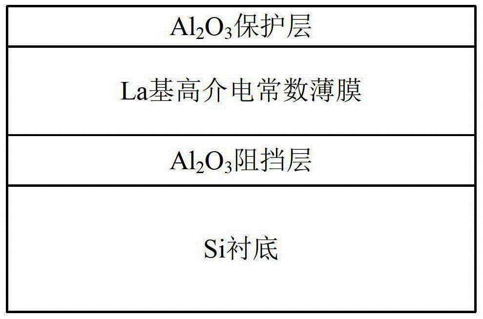
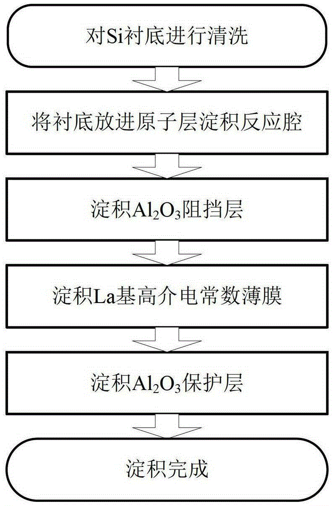
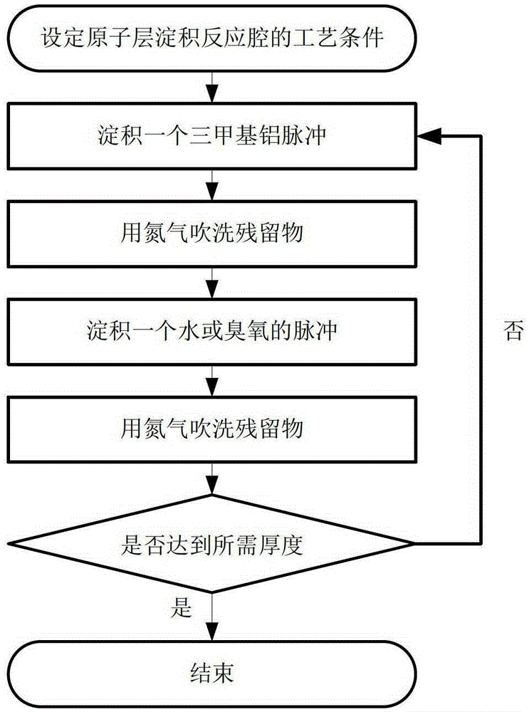
[0047] Example 1, preparation of Al 2 o 3 \La 2 o 3 \Al 2 o 3 \Si high dielectric constant gate dielectric material

[0048] Step 1, cleaning the silicon substrate.

[0049] 1a) Clean the Si sheet in SC-1 solution heated to 75°C for 10 minutes, the composition of the solution is NH 4 OH, H 2 o 2 and H 2 O, its ratio is 5:1:1, the main effect of this cleaning is to rely on NH 4 Complexation of OH with H 2 o 2 Strong oxidizing ability to remove organic pollutants or attached particles on Si wafers;

[0050] 1b) Rinse the Si sheet after cleaning in the SC-1 solution in deionized water for 2 minutes to remove the residual SC-1 solution;

[0051] 1c) Wash the Si sheet for 60 seconds in an HF solution consisting of HF and H 2 O, whose ratio is 1:50, the main function of this cleaning is to remove the natural oxide layer SiO on the surface of the Si substrate 2 ;

[0052] 1d) Rinse the Si sheet in deionized water to remove residual HF solution;

[0053] 1e) Place the...

example 2

[0074] Example 2, preparation of Al 2 o 3 \LaAlO 3 \Al 2 o 3 \Si high dielectric constant gate dielectric material

[0075] Step 1, cleaning the silicon substrate.

[0076] 1.1) Clean the Si sheet in an SC-1 solution heated to a temperature of 75°C for 10 minutes to remove organic pollutants or attached particles on the Si sheet. The composition of the solution is NH 4 OH, H 2 o 2 and H2 O, the ratio of which is 5:1:1;

[0077] 1.2) Rinse the Si sheet after cleaning with SC-1 solution in deionized water for 2 minutes to remove residual SC-1 solution;

[0078] 1.3) Clean the rinsed Si sheet in HF solution for 60 seconds to remove the natural oxide layer SiO on the surface of the Si substrate. 2 , the composition of the solution is HF and H 2 O, its ratio is 1:50;

[0079] 1.4) The natural oxide layer SiO on the surface of the Si substrate will be removed 2 The Si sheet is then rinsed in deionized water to remove residual HF solution;

[0080] 1.5) Place the Si shee...

example 3

[0103] Example 3, preparation of Al 2 o 3 \HfLaO\Al 2 o 3 \Si high dielectric constant gate dielectric material

[0104] Step A, cleaning the silicon substrate.

[0105] Clean the Si sheet in SC-1 solution heated to 75°C for 10 minutes to remove organic pollutants or attached particles on the Si sheet. The composition of the solution is NH 4 OH, H 2 o 2 and H 2 O, the ratio is 5:1:1; then rinse the Si sheet in deionized water for 2 minutes in SC-1 solution to remove residual SC-1 solution; then wash the Si sheet in HF and H 2 O ratio of 1:50 in the HF solution for 60 seconds to remove the natural oxide layer SiO on the surface of the Si substrate 2 ; The natural oxide layer SiO on the surface of the Si substrate will be removed 2 Then rinse the Si sheet in deionized water to remove the residual HF solution; place the Si sheet with the remaining HF solution in deionized water and use ultrasonic cleaning for 5 minutes to remove the adsorption particles on the surface, a...


PUM

PropertyMeasurementUnit
thicknessaaaaaaaaaa
thicknessaaaaaaaaaa
thicknessaaaaaaaaaa

Abstract

The invention discloses a gate dielectric material based on a silicon substrate high dielectric constant and a preparation method for the gate dielectric material, and mainly solves the problem that the conventional material is low in dielectric constant, low in thermal stability and low in film density. The gate dielectric material comprises a barrier layer (1), a La-based high dielectric constant film (2) and a protection layer (3) from the bottom to the top, wherein the barrier layer (1) adopts Al2O3 with the thickness of 0.5 to 3 nm; the La-based high dielectric constant film (2) adopts La2O3 or LaAlO3 or HfLaOx with the thickness of 1 to 10 nm; and the protection layer (3) adopts the Al2O3 with the thickness of 1 to 5 nm. The overall material is prepared by adopting an atomic layer deposition method. The gate dielectric material disclosed by the invention has the advantages of high dielectric constant, high film density, high step coverage, high thermal stability and low surface roughness, and can be used for manufacturing a gate dielectric film of a metal oxide semiconductor field effect transistor.

Description

technical field [0001] The invention belongs to the technical field of semiconductor materials, and particularly relates to a gate dielectric material with high dielectric constant based on a silicon substrate and a preparation method thereof, which can be used to manufacture gate dielectric films of metal oxide semiconductor field effect transistors. Background technique [0002] With the continuous reduction of the integration level of integrated circuits, the size of the metal oxide semiconductor field effect transistor MOSFET is continuously reduced, and the corresponding gate oxide thickness is also continuously reduced. As of 2008, 57nm lithography technology has become mature, and SiO2 as a gate dielectric film in high-performance field-effect transistor devices 2 The thickness of the layer has been reduced to less than 1nm. It is estimated that by 2014, the gate length will be reduced to 0.011μm, and the corresponding equivalent oxide layer thickness EOT should reach...

Claims


Application Information

Patent Timeline
Patent Type & Authority Patents(China)
IPC IPC(8): H01L29/51H01L21/285
Inventor 刘红侠费晨曦范小娇马飞樊继斌许韩晨玺
Owner XIDIAN UNIV
Learn More