
N-type diamond semiconductor monocrystal and production method thereof

A production method and diamond technology, applied in the direction of single crystal growth, single crystal growth, crystal growth, etc., can solve the problems of easy change of diamond crystal structure, increase of crystal internal resistance, slow growth rate of single crystal, etc., to achieve thermal conductivity and heat dissipation. The effect of good performance, increased number of free electrons, and extended chip life

Active Publication Date: 2013-05-15
焦作天宝桓祥机械科技有限公司
View PDF10 Cites 3 Cited by
  • Summary
  • Abstract
  • Description
  • Claims
  • Application Information

AI Technical Summary

Problems solved by technology

Japan's Sumitomo Corporation uses CVD (chemical vapor deposition) to synthesize N-type diamond semiconductors, using methane as a gas source and doping phosphorus atoms and sulfur atoms, and synthesizes N-type diamond semiconductors on (111) crystal-oriented substrates, but This process needs to use an expensive diamond single wafer as the substrate, and the speed of growing a single crystal is extremely slow, and the atomic radius of phosphorus and sulfur is much larger than that of carbon. This kind of doping can easily change the crystal structure inside the diamond, resulting in crystallization. lattice deformation, forming a large number of crystal defects, which will lead to an increase in the internal resistance of the crystal, and its actual performance will be greatly reduced

Method used


Image

  • N-type diamond semiconductor monocrystal and production method thereof
  • N-type diamond semiconductor monocrystal and production method thereof

Examples


Embodiment 1

[0033] Example 1: A kind of N-type diamond semiconductor single crystal, its production method comprises the following steps:

[0034] Accurately weigh 50kg of high-purity natural graphite powder and 50kg of iron-nickel alloy powder (iron-nickel ratio 7:3), place them in a three-dimensional mixer with a volume of 100 liters, add 0.5kg of lithium nitride powder, nitrogen 0.5kg of beryllium powder, seal the feeding port tightly, start the mixer, and mix the mixture for 10 hours to obtain a uniform mixture; wherein the particle size of the graphite powder is less than 200 mesh, the degree of graphitization is >95%, and the content of non-carbon impurities is less than 30ppm; The particle size of iron-nickel alloy powder is less than 200 mesh;

[0035] Put the mixture into a latex bag, let it stand for 20 minutes to exhaust; tie the mouth of the bag tightly, put it into a cold isostatic press and pressurize it to 300MPa, release the pressure after holding the pressure for 5 minu...

Embodiment 2

[0039] Example 2: A kind of N-type diamond semiconductor single crystal, production method comprises the following steps:

[0040] Accurately weigh 40kg of high-purity natural graphite powder and 60kg of nickel-manganese-cobalt alloy powder, wherein the mass ratio of nickel, manganese, and cobalt is 70:25:5; place graphite powder and alloy powder in a V-shaped mixing material with a volume of 100 liters In the mixer, add 1 kg of lithium nitride powder and 1 kg of beryllium nitride powder to the mixer, seal the feeding port tightly, and then start the mixer, and mix the materials for 15 hours to form a uniform mixture; wherein the particle size of the graphite powder is less than 200 mesh, The degree of graphitization is >95%; the particle size of the iron-nickel alloy powder is less than 200 mesh.

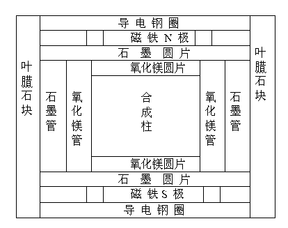
[0041] Put the mixture into a latex bag, let it stand for 20 minutes to exhaust, tie the mouth of the bag tightly, put it into a cold isostatic press, pressurize to 300 MPa, hold...

Embodiment 3

[0044] Example 3: A kind of N-type diamond semiconductor single crystal, its production method comprises the following steps:

[0045] Accurately weigh 55kg of high-purity natural graphite powder, 45kg of iron-nickel alloy powder (iron-nickel ratio 7:3), put them in a three-dimensional mixer with a volume of 100 liters, and then add 2.5kg of lithium nitride powder, Beryllium nitride powder 2.0kg, after sealing the feeding port, open the mixer, mix the materials for 18 hours, and obtain a uniform mixture; wherein the particle size of the graphite powder is less than 200 mesh, the degree of graphitization> 95%, and the particle size of the iron-nickel alloy powder is less than 200 mesh.

[0046] Put the mixture into a latex bag, let it stand for 20 minutes to exhaust air, tie the mouth of the bag tightly, put it into a cold isostatic press and pressurize it to 200MPa, release the pressure after holding the pressure for 6 minutes, and take out the pressurized material; The bul...


PUM

PropertyMeasurementUnit
sizeaaaaaaaaaa
particle sizeaaaaaaaaaa

Abstract

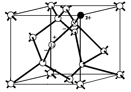
The invention relates to an N-type diamond semiconductor monocrystal and a production method thereof. The crystal contains nitrogen ions, lithium ions and beryllium ions regularly arrayed in the crystal, wherein the total content of nitrogen-lithium atom pairs, nitrogen-beryllium atom pairs and lithium-nitrogen-beryllium atom pairs is 100-10000ppm, the size of the semiconductor monocrystal is 0.3-10mm, and the crystal is a regular hexahedron, a regular octahedron or a hexahedron-octahedron. The production method comprises the following steps of: mixing graphite powder, a metal catalyst, lithium nitride and beryllium nitride in proportion, pressurizing to 100-300MPa to carry out cold isostatic pressing treatment, relieving the pressure, then breaking the mixed materials, placing the broken mixed materials into a mold to press to form columnar synthetic columns, sintering in vacuum, filling synthetic blocks, and processing in a high-temperature high-pressure oriented magnetic field; breaking the synthetic columns, performing electrolysis and separating by using a shaker to obtain the N-type diamond semiconductor monocrystal. The monocrystal provided by the invention is good in conductivity, high in optical-to-thermal energy conversion efficiency, suitable for manufacturing solar batteries, LED (Light Emitting Diode) sources and high-performance chips, and stable in performance.

Description

[0001] technical field [0002] The invention relates to a diamond semiconductor material, in particular to an N-type semiconductor diamond single crystal and a production method thereof. Background technique [0003] Traditional semiconductor materials are mainly silicon. With the further improvement of integrated circuit manufacturing technology, silicon semiconductor integrated circuits have entered the nanometer era. The integration of the latest Core i7 third-generation CPU chips has reached 22 nanometers. According to Moore's Law, the size of integrated circuits will be reduced by half every eighteen months, making the frequency of CPUs jump from hundreds of megabytes in the last century to gigabytes at present. However, as the manufacturing process of silicon semiconductor chips enters the nanometer era, the characteristics of silicon semiconductor materials have become the key to restricting the further improvement of chip performance. The operating temperature of co...

Claims


Application Information

Patent Timeline
Patent Type & Authority Applications(China)
IPC IPC(8): C30B29/04C30B1/12B01J3/06
Inventor 黄美玲
Owner 焦作天宝桓祥机械科技有限公司
Learn More