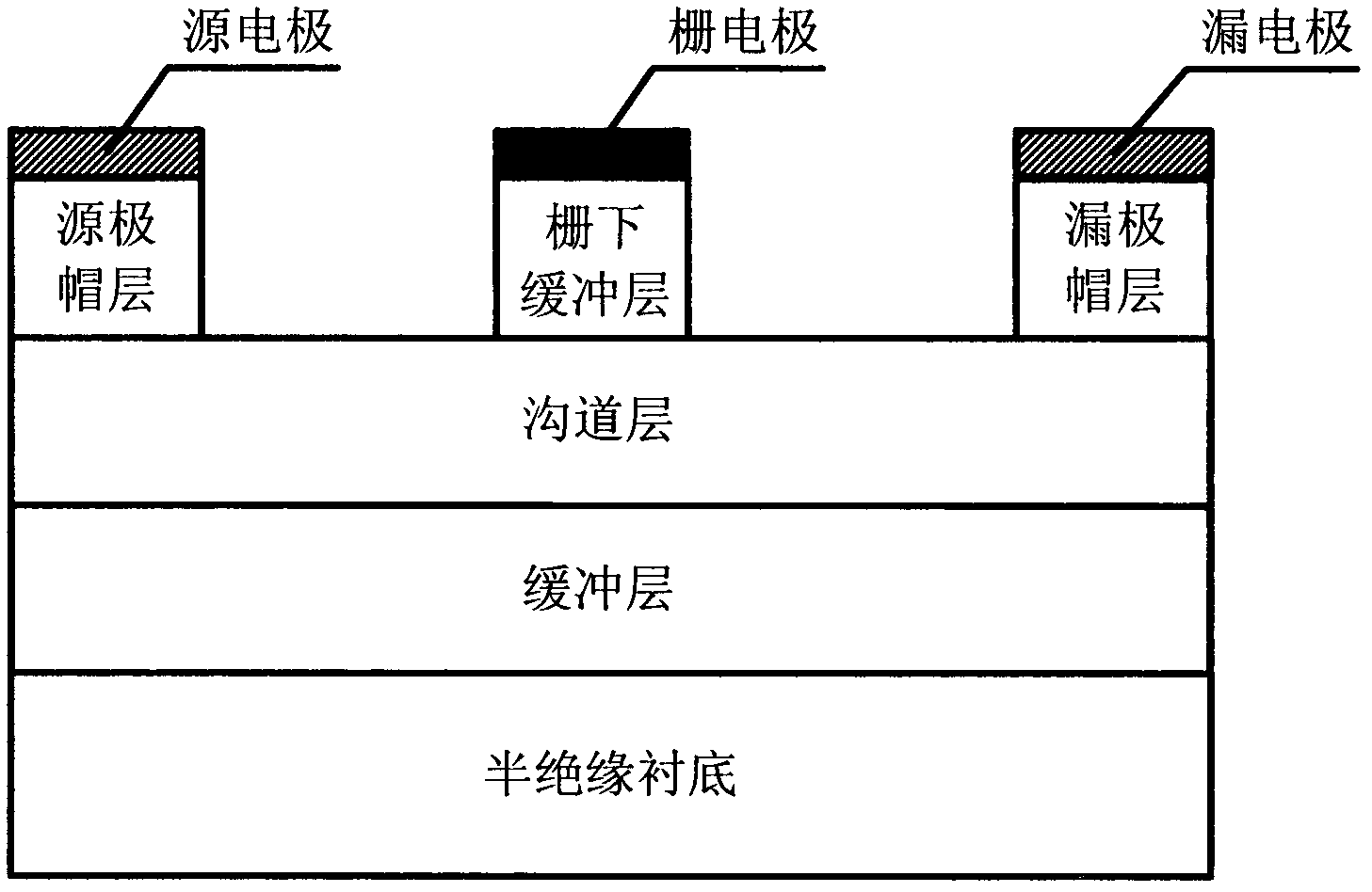
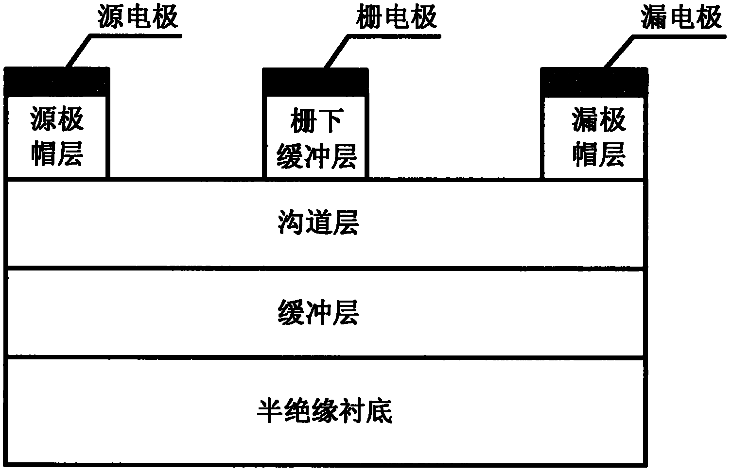
Metal-semiconductor field-effect transistor with gate lower buffer layer structure and manufacturing method
A field effect transistor, metal semiconductor technology, applied in the field of electronics, can solve the problems of the characteristic frequency and the highest oscillation frequency of the device, reduce the reliability of the device, affect the gain of the device, etc., so as to overcome the negative effects, improve the breakdown voltage, and improve the output. effect of current
- Summary
- Abstract
- Description
- Claims
- Application Information
AI Technical Summary
Problems solved by technology
Method used
Image

Examples
Embodiment 1
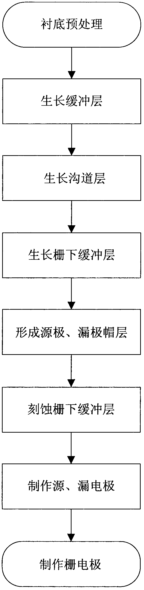
[0033] Embodiment 1, comprises the steps:
[0034] Step 1, substrate pretreatment.
[0035] Use acetone, methanol, and deionized water to clean the semi-insulating substrate sample in sequence, and then use the standard RCA cleaning process in the microelectronics process to remove impurities and oxide layers on the surface of the sample.
[0036] Step 2, growing the buffer layer.
[0037] On the front of the pretreated substrate sample, a homogeneous P-type buffer layer is grown by metal oxide semiconductor chemical vapor deposition. 15 cm -3 .
[0038] Step 3, growing a channel layer.
[0039] On the buffer layer, a homogeneous N-type channel layer is grown by metal oxide semiconductor chemical vapor deposition, with a thickness of 0.25 microns, phosphorus is used as impurity doping, and the doping concentration is 1.5×10 17 cm -3 .
[0040] Step 4, growing a buffer layer under the gate.
[0041] On the buffer layer, a homogeneous N-type buffer layer under the gate is ...
Embodiment 2
[0050] Embodiment 2, comprises the steps:
[0051] Step 1, substrate pretreatment.
[0052] Use acetone, methanol, and deionized water to clean the semi-insulating substrate sample in sequence, and then use the standard RCA cleaning process in the microelectronics process to remove impurities and oxide layers on the surface of the sample.
[0053] Step 2, growing the buffer layer.
[0054] On the front of the pretreated substrate sample, a homogeneous P-type buffer layer was grown by metal oxide semiconductor chemical vapor deposition. 15 cm -3 .
[0055] Step 3, growing a channel layer.
[0056] On the buffer layer, a homogeneous N-type channel layer is grown by metal oxide semiconductor chemical vapor deposition, with a thickness of 0.3 microns, phosphorus is used as doping impurity, and the doping concentration is 2.5×10 17 cm -3 .
[0057] Step 4, growing a buffer layer under the gate.
[0058] On the buffer layer, a homogeneous N-type buffer layer under the gate i...
Embodiment 3
[0067] Embodiment 3, comprises the steps:
[0068] Step 1, substrate pretreatment.
[0069] Use acetone, methanol, and deionized water to clean the semi-insulating substrate sample in sequence, and then use the standard RCA cleaning process in the microelectronics process to remove impurities and oxide layers on the surface of the sample.
[0070] Step 2, growing the buffer layer.
[0071] A homogeneous P-type buffer layer was grown on the front of the pretreated substrate sample by metal oxide semiconductor chemical vapor deposition. 15 cm -3 .
[0072] Step 3, growing a channel layer.
[0073] On the buffer layer, a homogeneous N-type channel layer is grown by metal oxide semiconductor chemical vapor deposition, with a thickness of 0.35 microns, phosphorus is used as impurity doping, and the doping concentration is 3.5×10 17 cm -3 .
[0074] Step 4, growing a buffer layer under the gate.
[0075] On the buffer layer, a homogeneous N-type buffer layer under the gate i...
PUM
 Abstract
Description
Claims
Application Information
 - R&D
- Intellectual Property
- Life Sciences
- Materials
- Tech Scout
- Unparalleled Data Quality
- Higher Quality Content
- 60% Fewer Hallucinations
Browse by: Latest US Patents, China's latest patents, Technical Efficacy Thesaurus, Application Domain, Technology Topic, Popular Technical Reports.
© 2025 PatSnap. All rights reserved.Legal|Privacy policy|Modern Slavery Act Transparency Statement|Sitemap|About US| Contact US: help@patsnap.com