Method and apparatus for improving the performance of a DAC switch array

a technology of dac switch array and performance improvement, which is applied in the direction of pulse manipulation, pulse technique, instruments, etc., can solve the problems of difficult design of high-performance dac system in low-power supply integrated circuit, and achieve the effect of reducing the voltage headroom of analog integrated circuits

Active Publication Date: 2014-05-06
TENSORCOM
View PDF8 Cites 1 Cited by
  • Summary
  • Abstract
  • Description
  • Claims
  • Application Information

AI Technical Summary

Benefits of technology

[0009]As the power supply voltage reduces in the scaling of integrated circuits, the voltage headroom for analog integrated circuits decreases correspondingly. This makes the design of high performance DAC systems in a low power supply integrated circuit much more challenging. Since each switch delivers a fixed voltage, the DAC dynamic performance is often evaluated by the maximum settling time regardless of the specific voltage level. Therefore, the same switch width for all voltage taps in the series coupled resistor network is not required.
[0010]In this embodiment, a tapered-switch width structure for a resistor ladder DAC is described. The p-channel transistor width is increased from 2 um to 5 um, in 4 consecutive groups to minimize layout concerns, as the tap voltage in the series coupled resistor network drops from 1.2 V to 0.7 V. Such structure minimizes the maximum settling time by keeping the switch parasitic capacitance minimum while maintaining relatively low on-resistance. This implementation proved to be very effective in simulation. A DAC with tapered switches settles within 0.1 LSB 50 pS faster than DAC with uniform-sized switches using a conventional implementation. A 50 pS improvement can have a profound advantage in a DAC operating at a clock rate of 2.64 GHz since the clock cycle time is only ˜380 pS.

Problems solved by technology

This makes the design of high performance DAC systems in a low power supply integrated circuit much more challenging.

Method used


Image

  • Method and apparatus for improving the performance of a DAC switch array
  • Method and apparatus for improving the performance of a DAC switch array
  • Method and apparatus for improving the performance of a DAC switch array

Examples


Embodiment Construction

[0031]The inventions presented in this specification can be used in any wired or wireless system, low power supply voltage design. The techniques are applicable to any DAC design.

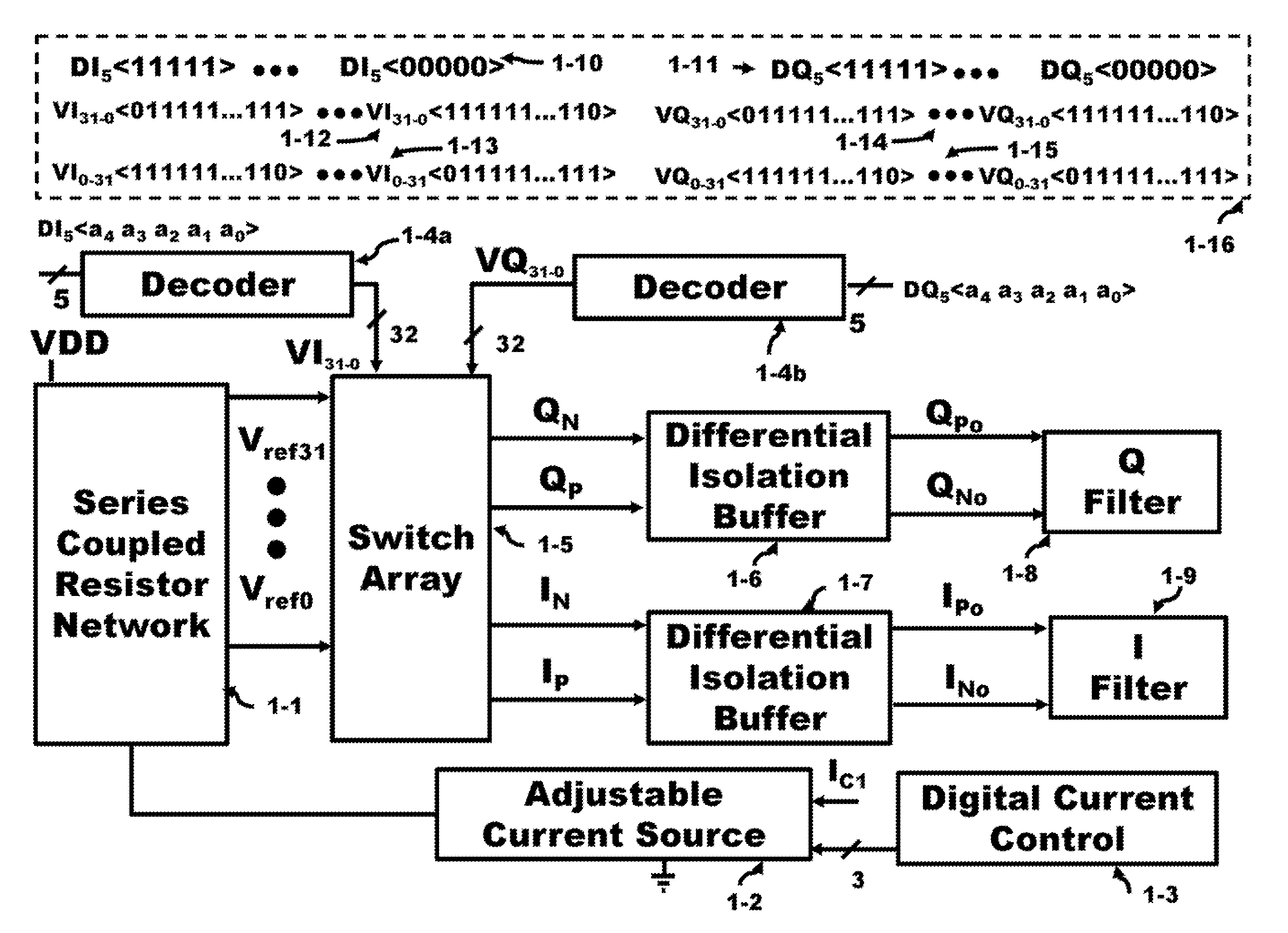
[0032]FIG. 1 illustrates a block diagram of the D / A converter and how the DAC output is applied to the I and Q filters. The two decoders 1-4a and 1-4b translate a 5 bit input into 32 bit patterns but the decoders could also be designed to operate on a 3 bit, 4 bit or other bit value input. At the top left is a decoder 1-4a receiving a five bit digital input for the I portion. The digital bits are DI54, a3, a2, a1, a0> providing 32 combinations. At the top right is a second decoder 1-4b receiving an additional five bit digital input for the Q portion. The digital bits are DQ54, a3, a2, a1, a0> providing 32 combinations. Examples of these strings are provided in box 1-16. The corresponding words for the input digital values DI5 and DI5 for VI31-0 is shown as 1-12 while corresponding words for the input digita...


PUM


Abstract

One of the critical design parameters occurs when a digital signal is converted into an analog signal. As the supply voltage drops to less than 2 times of threshold voltage to reduce leakage and save power, generating a relative large swing with a resistor-ladder DAC becomes more difficult. For a 5 bit DAC, 32 sub-arrays are used to select the appropriate voltage from the series coupled resistor network. Each sub-array uses p-channel transistors where the sub-array extracting the lowest voltage 700 mV only has a 100 mV of gate to source voltage. To compensate for the reduced gate to source voltage, the sub-arrays are partitioned into four groups. In each group, the p-channel width is increased from 2 um to 5 um, as the tap voltage drops from 1.2 V to 0.7 V. This allows the p-channel transistor with a small gate to source voltage to have a larger width thereby improving performance.

Description

BACKGROUND OF THE INVENTION[0001]The Federal Communications Commission (FCC) has allotted a spectrum of bandwidth in the 60 GHz frequency range (57 to 64 GHz). The Wireless Gigabit Alliance (WiGig) is targeting the standardization of this frequency band that will support data transmission rates up to 7 Gbps. Integrated circuits, formed in semiconductor die, offer high frequency operation in this millimeter wavelength range of frequencies. Some of these integrated circuits utilize Complementary Metal Oxide Semiconductor (CMOS), Silicon-Germanium (SiGe) or GaAs (Gallium Arsenide) technology to form the dice in these designs. Since WiGig transceivers use DAC (Digital to Analog Converters), the reduced power supply impacts the performance of the DAC's.[0002]CMOS (Complementary Metal Oxide Semiconductor) is the primary technology used to construct integrated circuits. N-channel transistors and P-channel transistors (MOS transistor) are used in this technology which uses fine line technol...

Claims


Application Information

Patent Timeline
Patent Type & Authority Patents(United States)
IPC IPC(8): H03M1/78
CPCH01L25/00H03M1/66H03M1/765H03M1/06
Inventor DAI, DAI
Owner TENSORCOM
Why Eureka
Try Eureka