
Universal test fixture for high-power packaged transistors and diodes

a technology for semiconductor devices and test fixtures, applied in the field of semiconductor device testing, can solve the problems of high heat generation of high-power packaged transistors and diodes, difficult work, and difficult handling of power transistor dies, etc., and achieves excellent thermal contact, maximum heat transfer, and high temperature resistance pressure

Inactive Publication Date: 2011-07-19
AESTECH
View PDF10 Cites 7 Cited by
  • Summary
  • Abstract
  • Description
  • Claims
  • Application Information

AI Technical Summary

Benefits of technology

Enables cost-effective, adaptable, and non-destructive testing of high-power packaged transistors and diodes across different package styles, reducing setup costs and preventing device damage, while maintaining optimal thermal and electrical performance.

Problems solved by technology

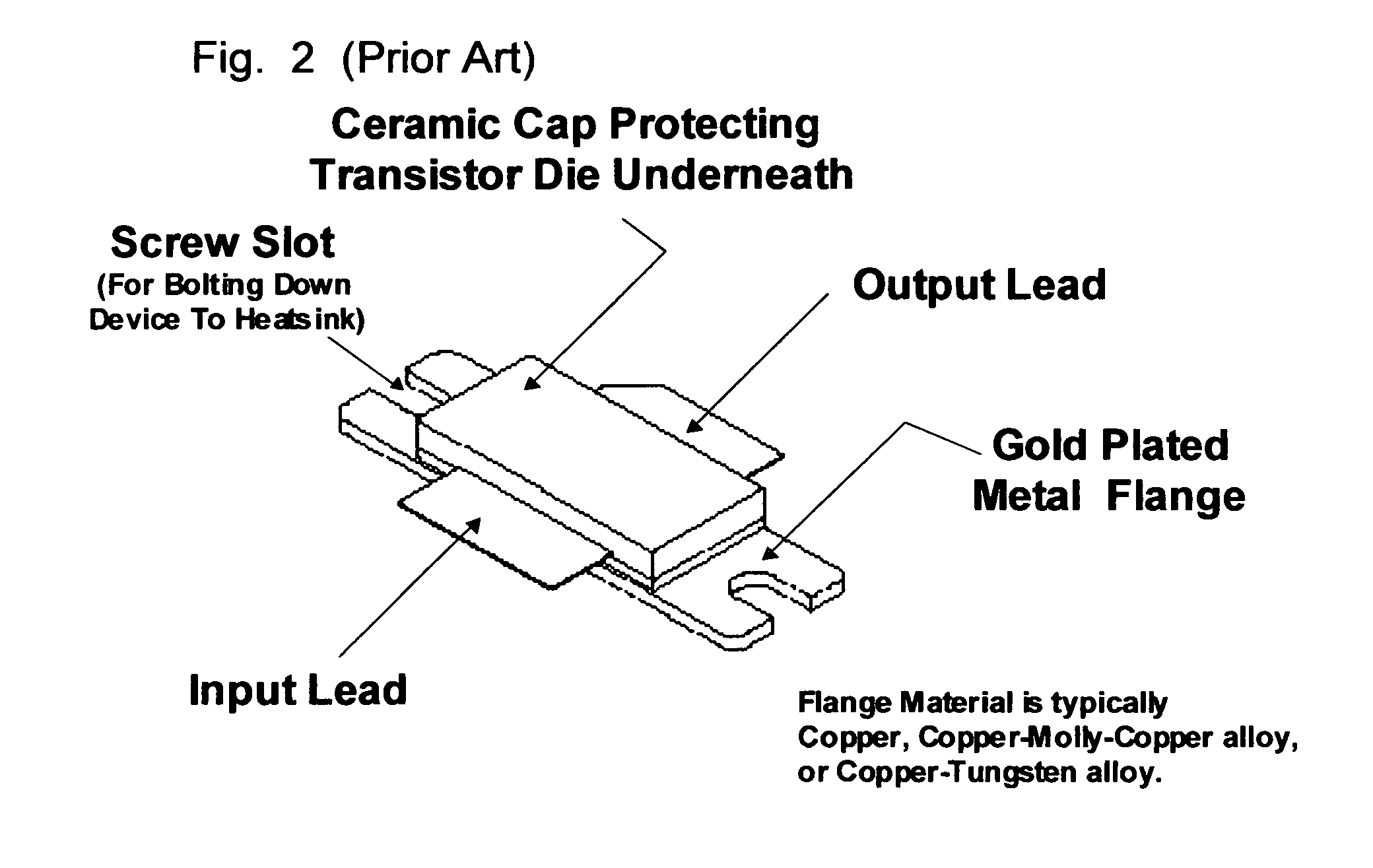
High-power RF and microwave transistor and diode chips are generally housed in expensive ceramic-metallic packages.
An RF power transistor die, sliced and cut from a wafer, exhibits very low impedance and is often very difficult to handle and work with when designing power amplifiers and oscillators, switches, and similar circuits.
Small size, special handling, and the need for ultra clean room to work with power transistor die and impedance variations are also among some of the reasons working with power transistor die can be difficult for a power amplifier designer.
High-power packaged transistors and diodes generate significant amounts of heat when used in high-power amplifiers, oscillators, attenuators, and the like.
For this reason, the high-power packaged transistors and diodes require adequate heat sinking to quickly remove the heat therefrom otherwise the temperature could rise above the maximum allowable junction temperature of the transistor or diode, resulting in degradation of the specified electrical performance, or even the destruction, of these expensive semiconductor components.
Since these devices generate a significant amount of heat when they are operated, a test fixture is required to have the ability to transfer heat away from the devices.
Once the custom model shop test fixture is completed, it cannot be used with devices having package styles other than the one for which it was originally designed.
This situation is often accompanied by long model shop lead times, expensive set up charges, the need for mechanical drawings, and so on.

Method used


Image

  • Universal test fixture for high-power packaged transistors and diodes
  • Universal test fixture for high-power packaged transistors and diodes
  • Universal test fixture for high-power packaged transistors and diodes

Examples


Embodiment Construction

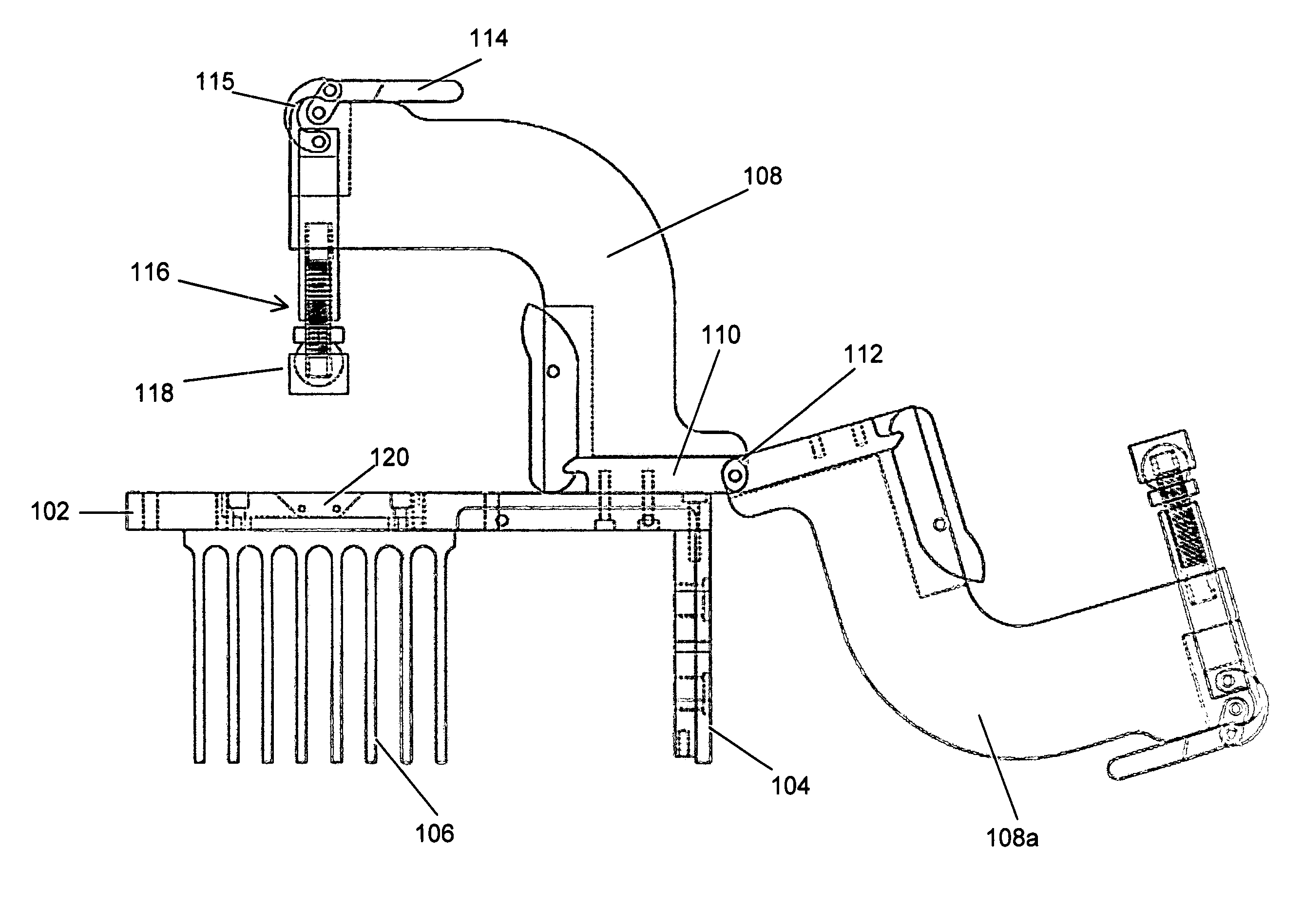
[0016]Generally, an apparatus in accordance with the present invention is provided that is suitable for receiving and holding, at one time, one or more high-power packaged transistors, diodes and the like; providing controlled impedance pathways between device under test and external circuitry, including but not limited to, test, evaluation, and characterization equipment; and operable to provide thermal conduction for at least heat removal purposes. The apparatus in accordance with the present invention is operable to accept a wide variety of package types, thus providing a common platform for operating a wide variety of high-power packaged semiconductor devices, including but not limited to, RF and microwave transistors and diodes, where those packages have a correspondingly wide variety of styles, shapes, geometries, and dimensions.

[0017]Characterization of RF power transistors, may include determination of beta, early voltage, emitter / base capacitance, frequency response, Ft, un...


PUM


Abstract

A universal test fixture for testing and characterization of high-power flange-packaged RF and microwave transistors and diodes includes a precision-machined heat sink having a built-in center cavity with a finger catch on either side of the cavity which uses a plurality of matching modules that are installed in the center cavity and designed as transistor or diode carrier modules to provide mounting for the high-power packaged RF and microwave devices in a wide variety of flange type packages, an adjustable clamping structure connected to a movable arm, and a plurality of non-conductive high temperature pressure clamps. Each carrier module is made of a gold-plated rectangular aluminum block having a center cavity that is machined to the package outline. A non-conductive black-anodized high-temperature resistant pressure clamp machined to the package outline holds the packaged device in the carrier module. When clamped down using the clamping structure, the pressure clamp holds the package leads on a printed circuit board ensuring excellent electrical contact between package leads and circuit traces and surrounding ground planes, obviating soldering and desoldering the leads to the circuit board. The pressure clamp also produces pressure along the device package to hold the packaged device to the carrier module which houses the device and which itself is bolted to the heat sink resulting in excellent thermal contact under the device.

Description

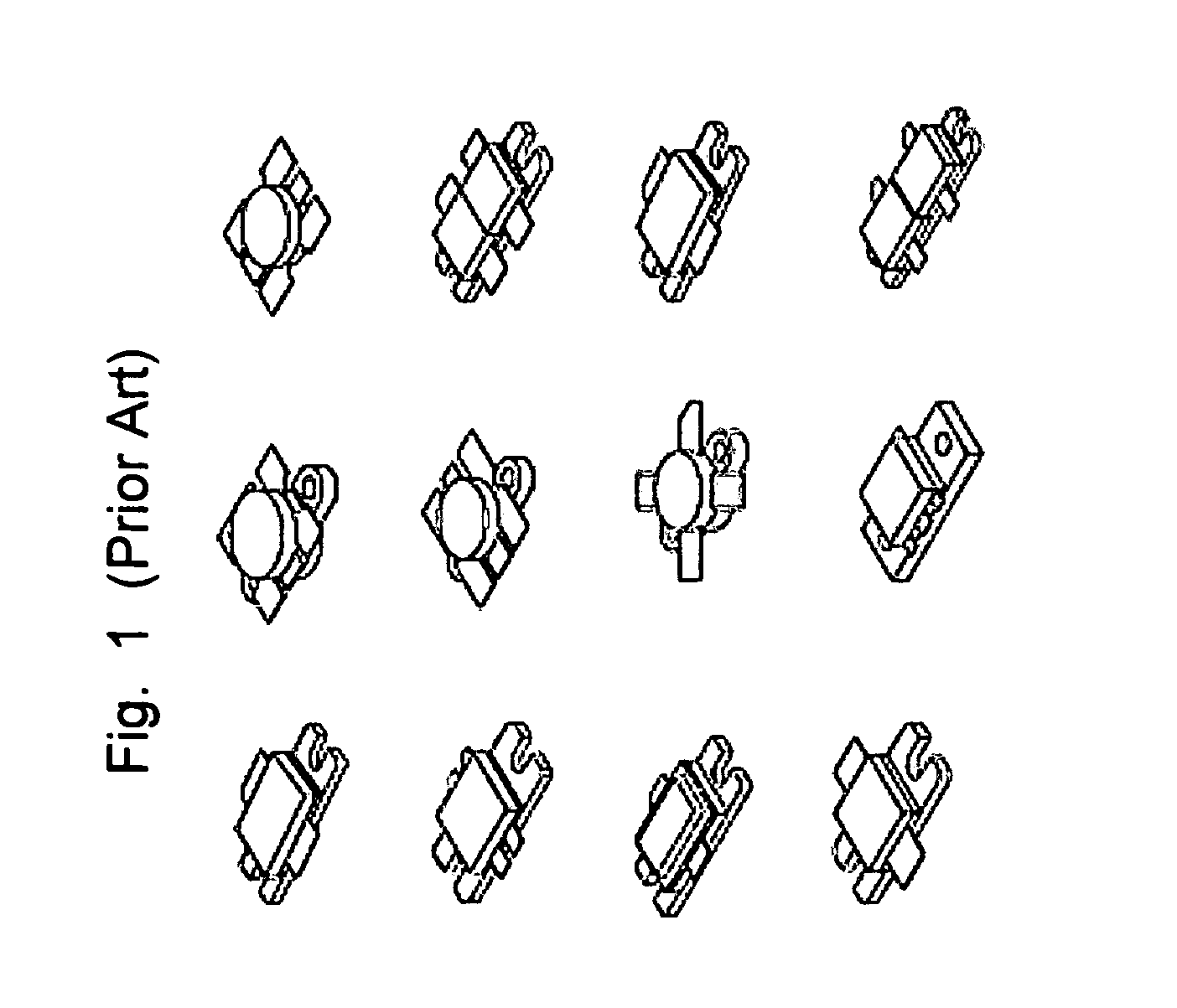
FIELD OF INVENTION[0001]The present invention relates generally to the field of semiconductor testing, and more particularly relates to a test fixture for high-power packaged semiconductor devices such as transistors and diodes used, for example, in RF or microwave applications.BACKGROUND[0002]High-power RF and microwave transistor and diode chips are generally housed in expensive ceramic-metallic packages. These packages are typically flange type, and are available in a wide variety of styles as shown in FIG. 1. An RF power transistor die, sliced and cut from a wafer, exhibits very low impedance and is often very difficult to handle and work with when designing power amplifiers and oscillators, switches, and similar circuits. Small size, special handling, and the need for ultra clean room to work with power transistor die and impedance variations are also among some of the reasons working with power transistor die can be difficult for a power amplifier designer. To make handling sa...

Claims


Application Information

Patent Timeline
Patent Type & Authority Patents(United States)
IPC IPC(8): G01R31/10G01R31/26
CPCG01R1/045G01R31/2601
Inventor GHADAKSAZ, MICHAEL M.
Owner AESTECH
Learn More