Method for manufacturing semiconductor device using quadruple-layer laminate

a semiconductor and quadruple-layer technology, applied in the direction of photosensitive materials, photomechanical devices, instruments, etc., can solve the problem of difficult to apply materials for organic-based anti-reflective films on substrates having a high aspect ratio, and the influence of actinic ray reflection on semiconductor substrates has become a serious problem, so as to improve the focus depth margin of a photoresist

Active Publication Date: 2010-11-30
NISSAN CHEM IND LTD
View PDF41 Cites 6 Cited by
  • Summary
  • Abstract
  • Description
  • Claims
  • Application Information

AI Technical Summary

Benefits of technology

[0033]In a method for manufacturing a semiconductor device according to the present invention including laminating each layer of an organic underlayer film (layer A), a silicon-containing hard mask (layer B), an organic antireflective film (layer C) and a photoresist film (layer D) in this order on a semiconductor substrate, at least four layers described above are laminated. In the micro processing using a KrF excimer laser (wave length: 248 nm), an ArF excimer laser (wave length: 193 nm), and the like, since a wiring width becomes narrow, pattern collapse of a photoresist (or simply referred to as a resist) occurs. In order to avoid the pattern collapse of the resist, a thickness of the resist layer has become thinner with decrease of the wiring width. When such a thin resist film is used, the dry etching rate of the resist underlayer film is also required to be further enhanced. However, for an organic based resist underlayer film to an organic based resist, a dry etching gas (for example, a fluorine type gas or oxygen gas) for the organic based resist underlayer film causes decrease of a thickness of the organic based resist film. On the other hand, in the case of a silicon-containing hard mask layer is used for a foundation layer of an organic based resist film, when the silicon-containing hard mask (layer B) is dry etched with a fluorine type gas, decrease of a thickness of the organic based resist film (resist-pattern formed resist film (layer D)) is small in the case of using a fluorine type gas. As a result, the resist pattern according to the thin resist film can be precisely transferred to the silicon-containing hard mask (layer B). Furthermore, when the organic underlayer film (layer A) is dry etched with an oxygen-type dry etching gas, decrease of a thickness of the silicon-containing hard mask (layer B) is small and the resist pattern can be precisely transferred to the organic underlayer film (layer A). A semiconductor substrate can be processed with a fluorine type gas by using the organic underlayer film (layer A) to which the resist pattern is transferred.
[0034]However, a triple-layer laminate formed by laminating an organic underlayer film (layer A), a silicon-containing hard mask (layer B), and a resist film (layer D) in this order on a semiconductor substrate as described above has two problems. One is that adherence between the silicon-containing hard mask (layer B) and the resist film (layer D) thereon is not sufficient. The other problem is that a resist shape is not formed in rectangle, because acid generated from a photoacid generator during exposure of the resist film is diffused into the silicon-containing hard mask (layer B). In the manufacture of a semiconductor device using such a triple-layer laminate, the above-described problems can be solved in a manner that an organic antireflective film (layer C) is disposed between the silicon-containing hard mask (layer B) and the resist film (layer D). That is, the adherence between the organic antireflective film (layer C) and the resist film (layer D) is significantly improved in a manner that the organic antireflective film (layer C) is made to have a chemical structure that is quite similar to the resist film (for example, a polymer of the organic antireflective film (layer C) has benzene rings or lactone rings which are specific for a polymer of the resist film (layer D)), and whereby a focus depth margin during exposure of the resist film can be significantly improved. In addition, the diffusion of an acid generated from a photoacid generator during exposure of the resist film to the silicon-containing hard mask (layer B) can be prevented in a manner that the organic antireflective film (layer C) is disposed between the silicon-containing hard mask (layer B) and the resist film (layer D). As a result, a resist pattern can be formed in rectangle. Moreover, since the organic antireflective film (layer C) is thinner than the organic underlayer film (layer A) or the silicon-containing hard mask (layer B), the decrease of a thickness of the resist film does not occur when the resist film (layer D) in which the resist pattern is formed is dry etched (for example, a dry etching using a fluorine type gas or oxygen gas), and the resist pattern can be precisely transferred to the organic antireflective film (layer C).
[0035]According to the present invention, processing of a semiconductor substrate having a fine wiring width becomes possible by using such a quadruple-layer laminate.BEST MODES FOR CARRYING OUT THE INVENTION
[0036]The present invention includes a method for manufacturing a semiconductor device by using a laminate including each layer of an organic underlayer film (layer A), a silicon-containing hard mask (layer B), an organic antireflective film (layer C) and a photoresist film (layer D) in this order on a semiconductor substrate.
[0037]The organic underlayer film (layer A) used in the present invention is a layer including a polymer having aromatic condensed rings in a main chain or a side chain bonded to the main chain constituting the polymer. The aromatic condensed ring includes a naphthalene ring and an anthracene ring.
[0038]This organic underlayer film (layer A) is a layer including a polymer having naphthalene rings in a main chain or a side chain bonded to the main chain. Particularly, a layer including a polymer having naphthalene rings in the side chain bonded to the main chain is preferable.

Problems solved by technology

Along with this change, influence of reflection of actinic rays from a semiconductor substrate has become a serious problem.
However, it is difficult to apply materials for an organic-based antireflective film on a substrate having a high aspect ratio, and in recent years, materials with a particular emphasis on filling property or flattening property have been developed (see, for example, Patent Document 1, Patent Document 2, and Patent Document 3).

Method used


Image

  • Method for manufacturing semiconductor device using quadruple-layer laminate
  • Method for manufacturing semiconductor device using quadruple-layer laminate
  • Method for manufacturing semiconductor device using quadruple-layer laminate

Examples


synthesis example 1

Production of an Organic Antireflective Film (Layer C) Forming Composition

[0356]

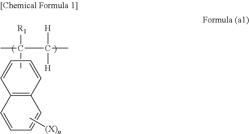
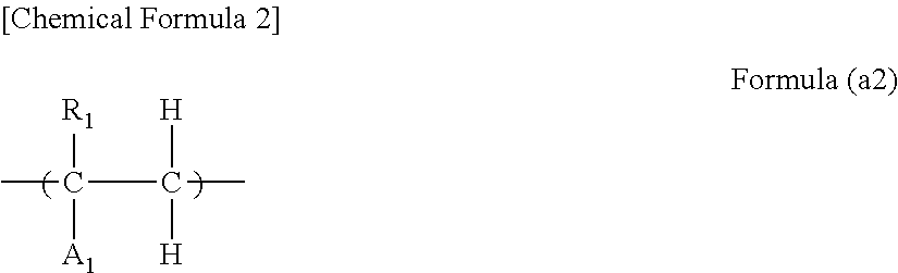
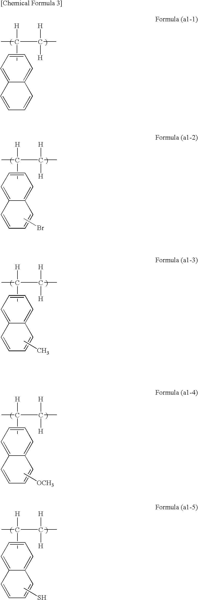
[0357]After 6.6 g (0.039 mole) of butyrolactone methacrylate of the above formula (1), 6.6 g (0.046 mole) of hydroxypropyl methacrylate and 6.8 g (0.039 mole) of benzyl methacrylate were dissolved in 64.4 g of tetrahydrofuran, an atmosphere in the flask was replaced with nitrogen and the temperature of the mixture was raised to the reflux temperature. After starting the reflux, 0.2 g of azo-bis-isobutyronitrile (AIBN) dissolved in 10 g of tetrahydrofuran were added under nitrogen pressure, and the mixture was reacted for 24 hours. After cooling the reaction solution, the solution was poured into diethyl ether to reprecipitate a polymer, and the polymer was dried by heating to obtain the resin of a formula (2). The obtained resin had a degree of polymerization of 490 and a weight average molecular weight (Mw) of 80000 (polystyrene conversion). A ratio of x:y1:y2 was 31%:38%:31% and a yield was 90%.

[0358]

[...

synthesis example 2

Production of a Silicon-Containing Hard Mask (Layer B) Forming Composition

[0360]4.00 g of phenyltrimethoxysilane, 10.99 g of methyltriethoxysilane, 15.35 g of tetramethoxysilane, 7.08 g of water and 0.365 g of p-toluenesulfonic acid were added to 40.71 g of propylene glycol monomethyl ether. The mixture was stirred for 1 hour at 80° C. to obtain the resin of a formula (3). In the formula (3), a ratio of S1:S2:S3 is 11%:33%:56%. The obtained polysiloxane resin in the formula (3) had a weight average molecular weight of 11000 and a number average molecular weight of 3400.

[0361]

[0362]Then, 0.195 g of p-toluenesulfonic acid, 2.68 g of propylene glycol monomethyl ether, 8.78 g of propylene glycol monomethyl ether acetate and 17.5 g of cyclohexanone were added to 10 g of the reaction solution having a concentration of solid content of 39% by mass to be a 10.0% by mass solution. The solution was filtrated by using a microfilter made of polyethylene having a pore diameter of 0.2 μm to obtai...

synthesis example 3

Production of a Silicon-Containing Hard Mask (Layer B) Forming Composition

[0363]5.0 g of a polysilane compound SI-2020 (manufactured by Osaka Gas Chemicals Co., Ltd., a weight average molecule weight: 5900, number average molecule weight: 1800, a ratio of X:Y in the polysilane of a formula (4) is 50%:50%, both terminals have silanol groups) having the unit structure of the formula (4),

[0364]

5.0 g of KN 030 (manufactured by Osaka Organic Chemical Industry Ltd., a component is a copolymer of naphthol novolac and cresol novolac, and a ratio of copolymer is naphthol novolac of 70 mol % and cresol novolac of 30 mol %, and a weight average molecule weight is 1500), and 2.50 g of tetramethoxymethyl glycoluryl and 0.125 g of pyridinium-p-toluenesulfonic acid were added to 114.5 g of propylene glycol monomethyl ether acetate to be a 10.0% by mass solution. The solution was filtrated by using a microfilter made of polyethylene having a pore diameter of 0.2 μm to prepare the solution of the si...


PUM


Abstract

There is provided a laminate used as an underlayer layer for a photoresist in a lithography process of a semiconductor device and a method for manufacturing a semiconductor device by using the laminate. The method comprising: laminating each layer of an organic underlayer film (layer A), a silicon-containing hard mask (layer B), an organic antireflective film (layer C) and a photoresist film (layer D) in this order on a semiconductor substrate. The method also comprises: forming a resist pattern in the photoresist film (layer D); etching the organic antireflective film (layer C) with the resist pattern; etching the silicon-containing hard mask (layer B) with the patterned organic antireflective film (layer C); etching the organic underlayer film (layer A) with the patterned silicon-containing hard mask (layer B); and processing the semiconductor substrate with the patterned organic underlayer film (layer A).

Description

TECHNICAL FIELD[0001]The present invention relates to a laminate used as an underlayer layer for a photoresist in a lithography process of a semiconductor device and a method for manufacturing a semiconductor device by using the laminate.BACKGROUND ART[0002]In the manufacture of a semiconductor device, micro processing by lithography using a photoresist has been performed. The micro processing is a processing method including forming a thin film of a photoresist on a semiconductor substrate such as silicon wafer, irradiating actinic rays such as ultra violet rays through a mask pattern on which a pattern for a semiconductor device is depicted to develop, and etching the substrate by using an obtained photoresist pattern as a protective film, thereby forming fine unevenness corresponding to the pattern on the surface of the substrate. However, in recent progress in high integration of semiconductor devices, shorter wavelength actinic rays tend to be used. For example, an ArF excimer ...

Claims


Application Information

Patent Timeline
Patent Type & Authority Patents(United States)
IPC IPC(8): H01L21/31
CPCG03F7/0752G03F7/091G03F7/11H01L21/31144H01L21/0332H01L21/31138H01L21/0274G03F7/161H01L21/0276
Inventor TAKEI, SATOSHINAKAJIMA, MAKOTOSAKAIDA, YASUSHIIMAMURA, HIKARUHASHIMOTO, KEISUKEKISHIOKA, TAKAHIRO
Owner NISSAN CHEM IND LTD
Why Eureka
Try Eureka