Room temperature hydrogen sensor
a hydrogen sensor and room temperature technology, applied in the field of room temperature hydrogen sensors, can solve the problems of affecting the electrical resistance characteristics of the measuring circuit, requiring the utilization of robust safety devices for hydrogen, and raising the temperature of beads, etc., and achieves the effect of large dynamic detection range and easy incorporation
- Summary
- Abstract
- Description
- Claims
- Application Information
AI Technical Summary
Benefits of technology
Problems solved by technology
Method used
Image
Examples
example 1
MEMS Based Sensor Platform Fabrication
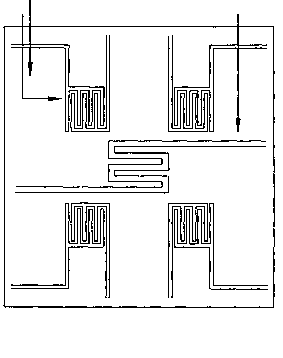
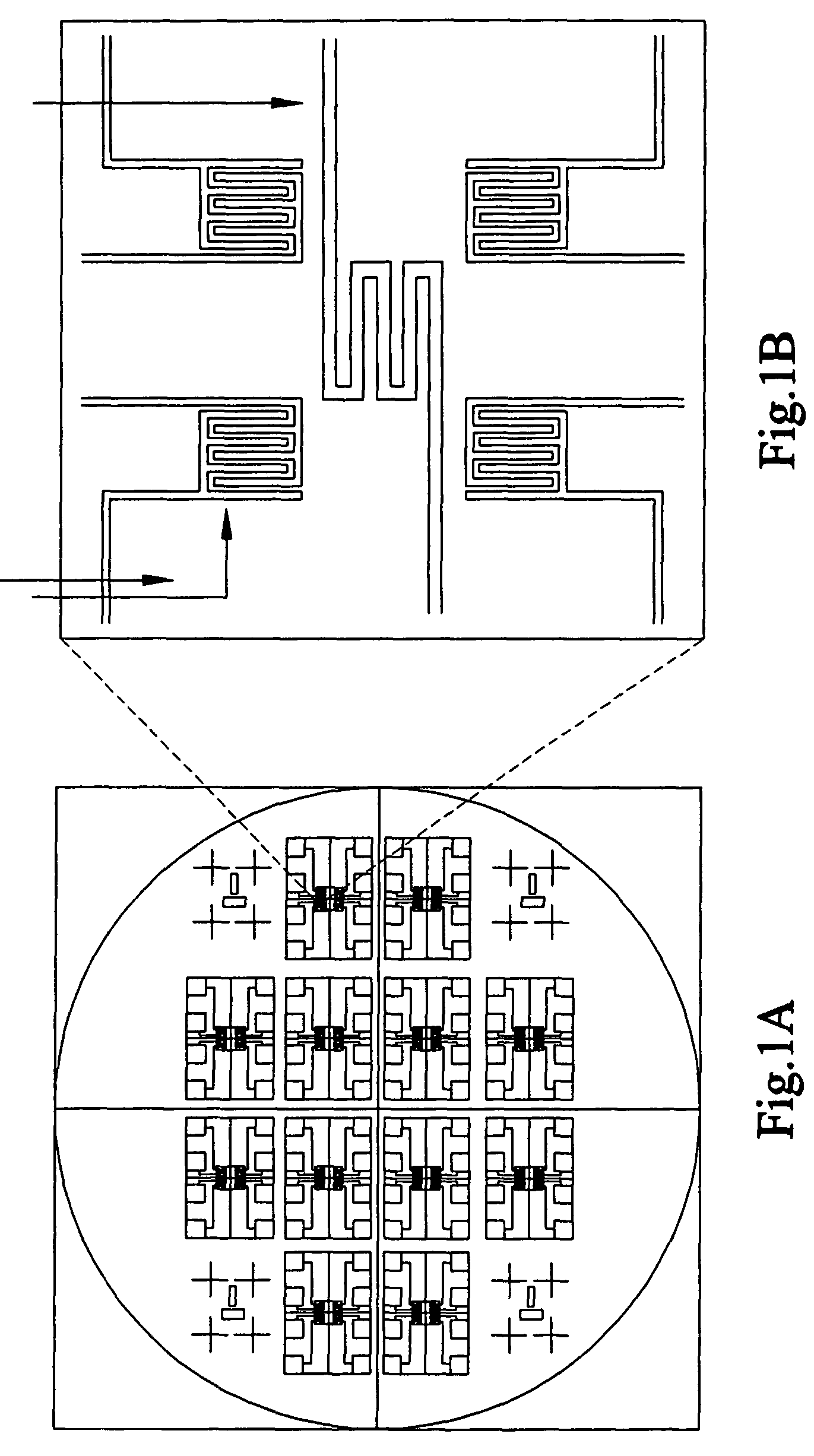
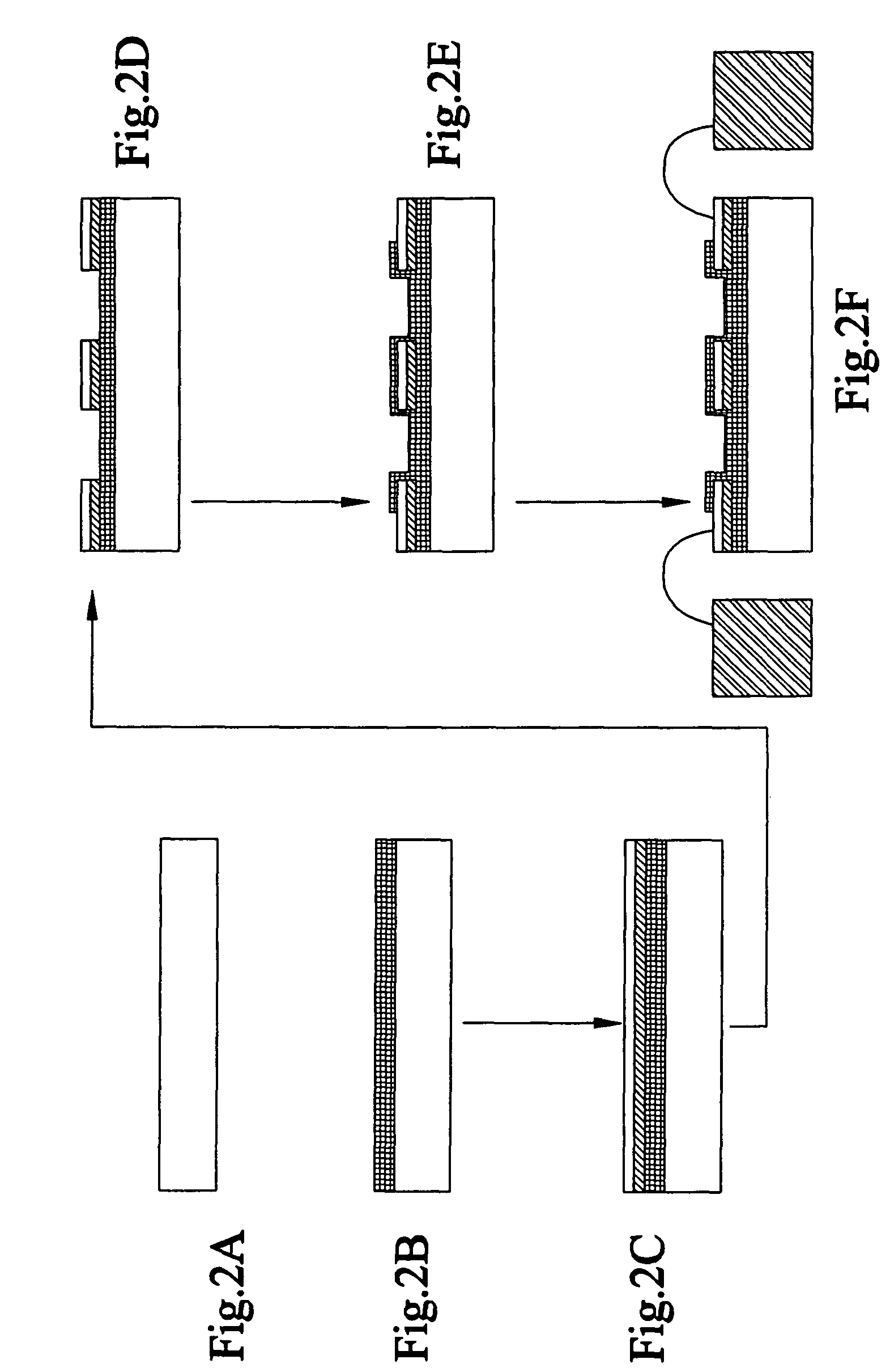
[0086]A 3″ Si (100) wafer is used as a substrate for sensor fabrication. On top of the substrate 0.1 to 1 mm of silicon oxide is thermally grown. Alternatively, oxide can be deposited by other methods such as CVD or sputtering. Oxide is used as an insulation layer. Alternatively, glass substrate can be used. 10-50 nm-thick chromium (Cr) or titanium (Ti) and 100-500 nm-thick gold (Au) films are deposited by thermal or e-beam evaporation on top of the oxide layer or on the glass substrate. The interdigitated electrodes were patterned on the substrate using photolithography and wet chemical etching. Positive or negative photoresist was used for patterning the electrodes. Alternatively, a lift-off method is used to pattern the electrodes. The gap between electrodes is kept in the range of 10 nm to 50 mm. After sol-gel coating of In2O3 doped-SnO2 thin films over the sensor platform, in which coating process is outlined in the following section, the M...
example 3
Fabrication of a MEMS Based Hydrogen Sensor
[0089]Micro structures were fabricated through a commercial foundry and the as-received die was micro machined using XeF2 as a silicon selective etchant. A photolithographic lift-off process was used in combination with physical vapor deposition (PVD) to sequentially deposit a gold / titanium thin film overlaid by a indium oxide doped tin oxide on the suspended micro structures. The resulting devices were wire bonded and packaged in 40 pin ceramic chip carriers.
[0090]The fully packaged chips were placed in a sealed chamber, and electrical contact made via feedthroughs into the chamber. Nitrogen and hydrogen were introduced into the chamber and controlled with mass flow controllers and actuated valves. The resistance of the sensing film was measured periodically with a digital multimeter and logged on a desktop computer.
PUM
 Abstract
Description
Claims
Application Information
 - R&D
- Intellectual Property
- Life Sciences
- Materials
- Tech Scout
- Unparalleled Data Quality
- Higher Quality Content
- 60% Fewer Hallucinations
Browse by: Latest US Patents, China's latest patents, Technical Efficacy Thesaurus, Application Domain, Technology Topic, Popular Technical Reports.
© 2025 PatSnap. All rights reserved.Legal|Privacy policy|Modern Slavery Act Transparency Statement|Sitemap|About US| Contact US: help@patsnap.com


