Conjugated molecule and electroluminescent device thereof and electronic device having the electroluminescent device
a technology of conjugated molecules and electroluminescent devices, which is applied in the field of display devices, can solve the problems of difficult chemical modification of compounds and remarkably low solubility of phthalocyanines, and achieve excellent hole injection characteristics, small redox potential, and small absorption in visible regions.
- Summary
- Abstract
- Description
- Claims
- Application Information
AI Technical Summary
Benefits of technology
Problems solved by technology
Method used
Image
Examples
embodiment mode 1
(Embodiment Mode 1)
[0042]In this embodiment mode, a structure of a compound suitable for carrying out this invention will be described. In the compound represented by the general formula [Chem. 5], X and Z may be the same or different and represent a sulfur atom, an oxygen atom, or a nitrogen atom or a silicon atom each having an alkyl group or an arylen group. The alkyl group on the nitrogen atom or the silicon atom is an aliphatic hydrocarbon group having 1 to 4 carbon atoms (a methyl group, an ethyl group, a propyl group, an isopropyl group, a sec-butyl group, a tert-butyl group, etc.) or an aliphatic cyclic hydrocarbon group having 4 to 6 carbon atoms (a cyclobutyl group, a cyclopentyl group, a cyclohexyl group, etc.). The aryl group on the nitrogen atom or the silicon atom is an aromatic group such as a phenyl group, a naphthyl group, an anthranyl group, and a prenyl group, in each of the aromatic groups a hydrogen atom may be substituted by a hydrocarbon group or an alkoxy gro...
embodiment mode 2
(Embodiment Mode 2)
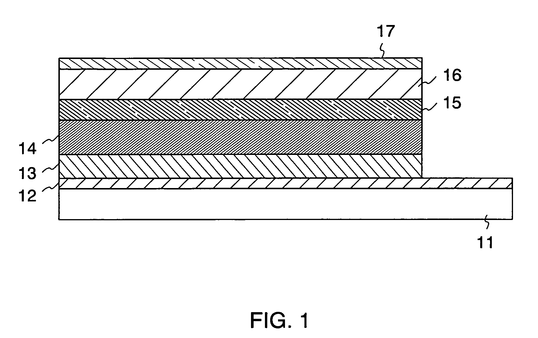
[0047]In this embodiment mode, a basic structure of an electroluminescent device using the compounds represented by the general formulas [Chem. 5] to [Chem. 8] will be described with reference to FIG. 1. A device structure described in this embodiment mode of the invention is such that, but not limited to, a hole injection layer, a hole transporting layer, a luminescent layer, and an electron transporting layer are provided between a cathode and an anode, and various electroluminescent device structures such as an anode / hole injection layer / luminescent layer / electron transporting layer / cathode, an anode / hole injection layer / hole transporting layer / luminescent layer / electron transporting layer / electron injection layer / cathode, an anode / hole injection layer / hole transporting layer / luminescent layer / hole blocking layer / electron transporting layer / cathode, an anode / hole injection layer / hole transporting layer / luminescent layer / hole blocking layer / electron transporting...
embodiment mode 3
(Embodiment Mode 3)
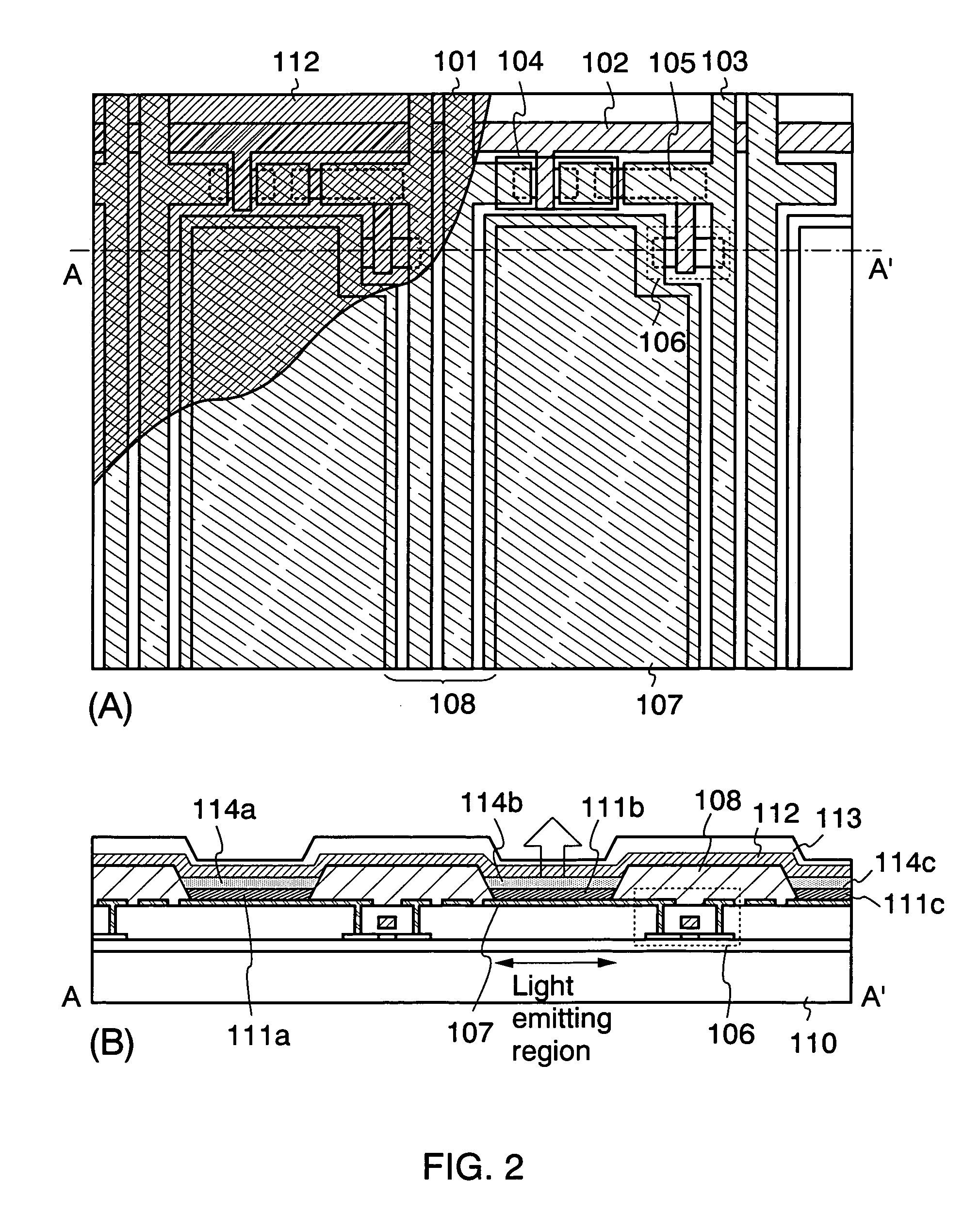
[0053]In this embodiment mode, an electroluminescence device to be manufactured on a substrate on which a TFT has been mounted will be described using FIG. 2.
[0054]In a pixel structure shown in FIG. 2(A), denoted by 101 is a data signal line; denoted by 102 is a gate signal line; denoted by 103 a power line; denoted by 104 is a TFT for switching (hereinafter referred to as a switching TFT); denoted by 105 is a condenser for charge retention; denoted by 106 is a TFT for driving (hereinafter referred to as a driving TFT) which serves to supply a current to the electroluminescent device; and denoted by 107 is a pixel electrode connected to a drain of the driving TFT, which functions as an anode of the light emitting device. Denoted by 112 is an opposed electrode which functions as a cathode of the light emitting device.
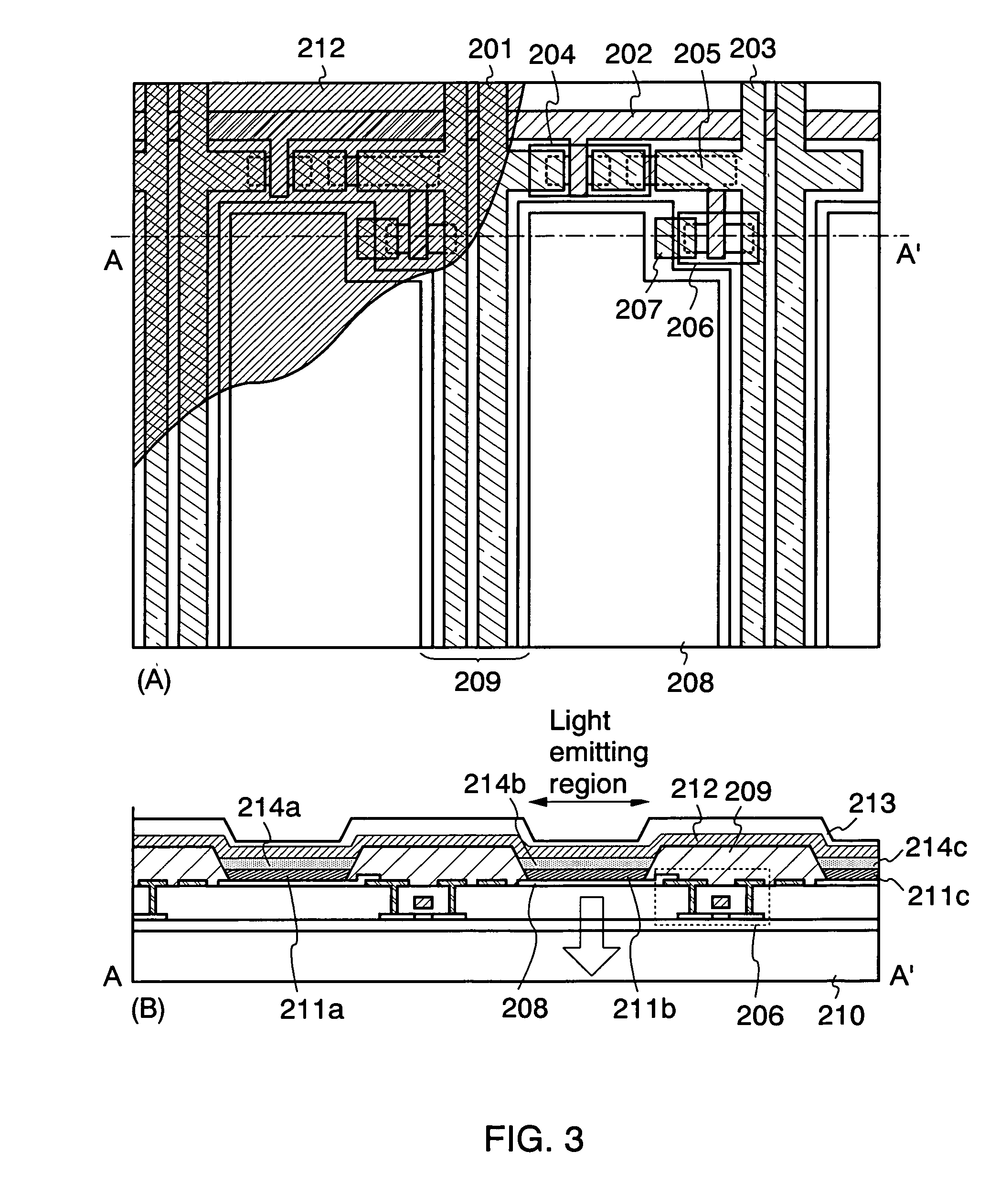
[0055]Shown in FIG. 2(B) is a diagram corresponding to a section indicated by the line A–A′. In FIG. 2(B), denoted by 110 is a substrate, and it is po...
PUM
| Property | Measurement | Unit |
|---|---|---|
| Temperature | aaaaa | aaaaa |
| Pressure | aaaaa | aaaaa |
| Solubility (mass) | aaaaa | aaaaa |
Abstract
Description
Claims
Application Information
 - R&D
- Intellectual Property
- Life Sciences
- Materials
- Tech Scout
- Unparalleled Data Quality
- Higher Quality Content
- 60% Fewer Hallucinations
Browse by: Latest US Patents, China's latest patents, Technical Efficacy Thesaurus, Application Domain, Technology Topic, Popular Technical Reports.
© 2025 PatSnap. All rights reserved.Legal|Privacy policy|Modern Slavery Act Transparency Statement|Sitemap|About US| Contact US: help@patsnap.com


