Manufacturing method of semiconductor device
a manufacturing method and semiconductor technology, applied in the direction of semiconductor devices, electrical devices, transistors, etc., can solve the problems of lowering the top surface of the buried insulating film with respect to the substrate surface plane, affecting the device performance, and affecting the device quality, etc., to suppress the plasma damage to the substrate surface, improve the device performance, and improve the effect of device performan
- Summary
- Abstract
- Description
- Claims
- Application Information
AI Technical Summary
Benefits of technology
Problems solved by technology
Method used
Image

Examples
first embodiment
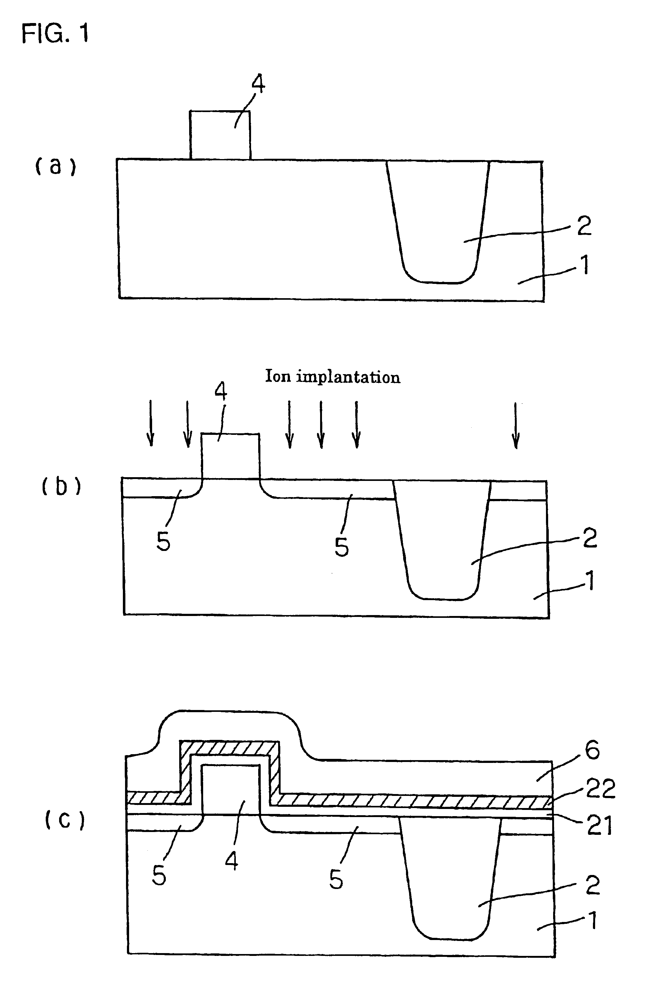
[0112]Referring to the drawings, the first embodiment of the present invention is described in detail. FIG. 1 to FIG. 3 are a series of schematic cross-sectional views illustrating the steps of a manufacturing method of a MOS transistor having a LDD structure.
[0113]First, in a prescribed region of a semiconductor substrate 1, a trench isolation region is formed by a known method, in which a silicon oxide film is buried.
[0114]On the silicon substrate 1, a gate insulator of a thermal oxidation film (not shown in the drawings) with a thickness from 2 nm to 15 nm is formed, and a doped polycrystalline silicon film with a thickness from 100 nm to 200 nm is subsequently formed on the gate insulator. By patterning this polycrystalline silicon film by lithography and etching, a gate electrode 4 is then formed (FIG. 1(a)). Hereat, a silicide film and a cap insulating film can be formed on the gate electrode by sputtering a silicide film such as a W silicide film on the doped polycrystalline ...
second embodiment
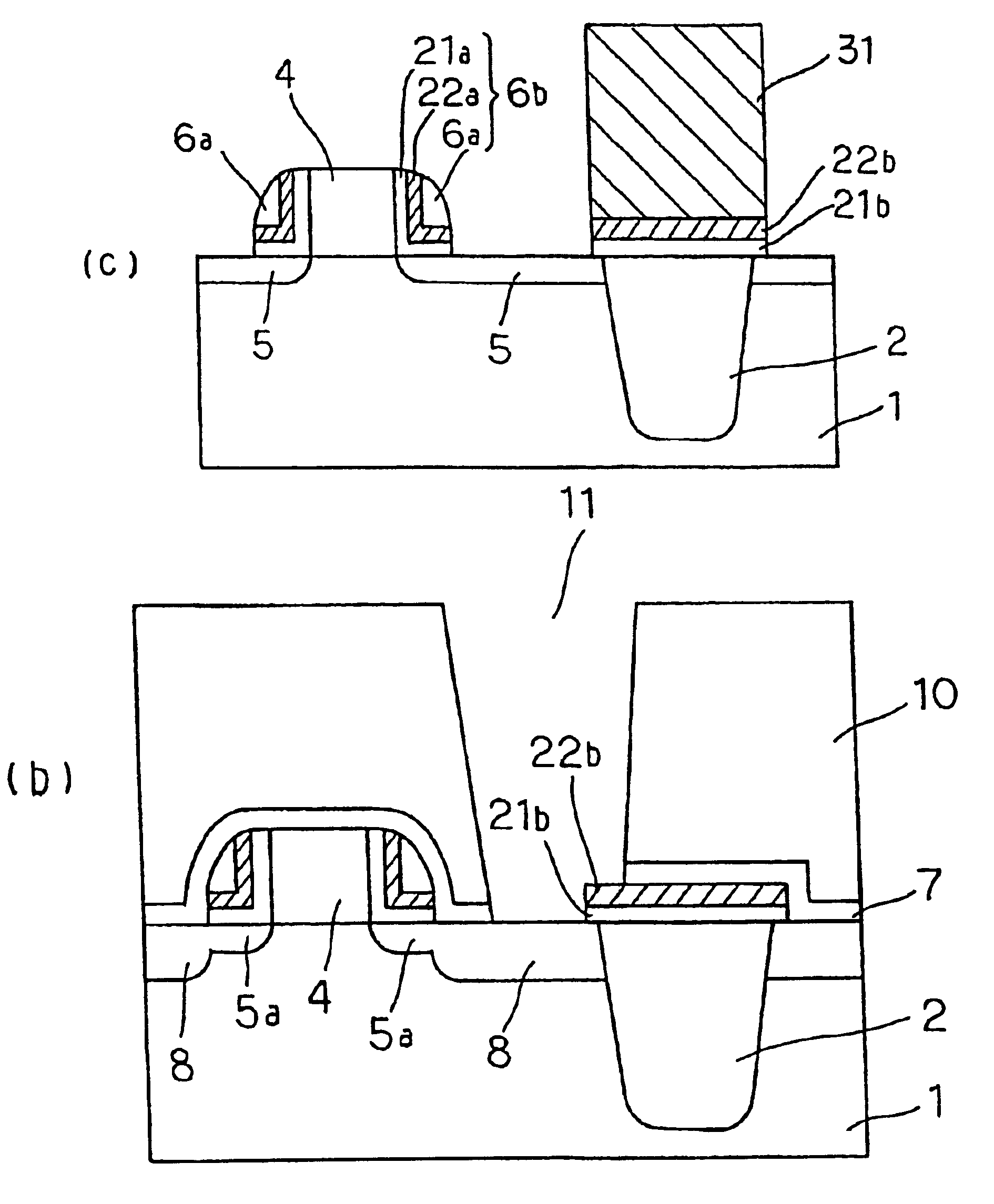
[0127]FIG. 4 to FIG. 5 are a series of schematic cross-sectional views illustrating the steps of the second embodiment of a manufacturing method according to the present invention. Hereat, FIG. 4(a) and FIG. 2(a) show the same drawing. A structure shown in FIG. 4(a) is formed in like manner as the steps shown from FIG. 1(a) to FIG. 2(a).
[0128]FIG. 4(b) shows that a resist film 31 is formed on the silicon nitride film 22 to cover the region above the trench isolation region 2. The pattern of a resist film 31 is same as the pattern of trench isolation region. Thus, in the patterning of the resist film 31, the same mask can be used as in the trench isolation region patterning.
[0129]Subsequently, the formation of sidewalls is performed by anisotropic etching to remove the silicon nitride film 22 and the silicon oxide film 21 and to expose the top surface of both the gate electrode 4 and the silicon substrate. As a result, the layered film of sidewalls 6b composed of the silicon oxide fi...
third embodiment
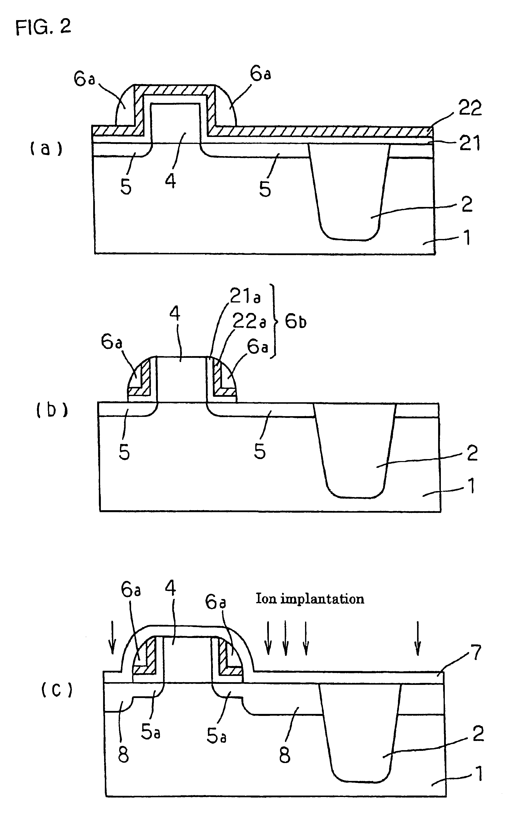
[0135]FIG. 6 to FIG. 8 are a series of schematic cross-sectional views illustrating the steps of the third embodiment of a manufacturing method according to the present invention.
[0136]As shown in FIG. 6(a), following that a trench isolation region buried with silicon oxide film is formed on the silicon substrate 1 by a known method, a gate insulator of a thermal oxidation film (not shown) and a doped polycrystalline silicon layer are formed and the gate electrode 4 is formed by patterning the polycrystalline silicon film.
[0137]Next, in the same way as the first embodiment, using the gate electrode 4 as a mask, an ion implantation is performed to form LDD regions 5 with low concentration of dopant and a conductive type with opposite to the one of the substrate (FIG. 6(b)).
[0138]Next, over the entire surface of the substrate, a silicon oxide film 6 with a thickness from 50 nm to 200 nm is formed, by the CVD method, to cover the gate electrode 4 (FIG. 6(c)), and then, by etching back ...
PUM
 Abstract
Description
Claims
Application Information
 - R&D
- Intellectual Property
- Life Sciences
- Materials
- Tech Scout
- Unparalleled Data Quality
- Higher Quality Content
- 60% Fewer Hallucinations
Browse by: Latest US Patents, China's latest patents, Technical Efficacy Thesaurus, Application Domain, Technology Topic, Popular Technical Reports.
© 2025 PatSnap. All rights reserved.Legal|Privacy policy|Modern Slavery Act Transparency Statement|Sitemap|About US| Contact US: help@patsnap.com