Near-field optical recording medium and near-field optical recording method
a near-field optical and recording medium technology, applied in the field of medium and a near-field optical recording method, can solve the problems of complex apparatus, difficult practical use, and the recording density achieved by these techniques has reached the maximum, and achieves the effect of sufficient durability and improved recording density
- Summary
- Abstract
- Description
- Claims
- Application Information
AI Technical Summary
Benefits of technology
Problems solved by technology
Method used
Image
Examples
preparation example 1
[0084]
[0085]To 1.4 g (2.99 mmol) of compound (i) was added 15 ml of nitrobenzene, the mixture cooled with ice-water, and 0.3 ml (3 mmol) of Cl2CHOCH3O added thereto. To the mixture was added 403 mg (3 mmol) of ground AlCl3. The mixture was extracted with chloroform. The extract was purified by column chromatography (eluent: hexane / chloroform=1:1) to give compound (ii) in a yield of 70%.
[0086]In 250 ml of benzene were dissolved 27.4 g (100 mmol) of bromidiphenylmethane and 28.8 g (110 mmol) of triphenylphosphine, and the mixture was heated under reflux for 16 hours. After allowing the reaction mixture to cool, the precipitate was collected by filtration to give compound (iii) as a white solid. The reaction yield was 30%.
[0087]In tetrahydrofuran was dissolved 1.06 g (2.09 mmol) of compound (iii), and 1.3 ml (2.09 mmol) of n-butyl lithium was added dropwise to the solution at 0° C. in an argon gas atmosphere. After the mixture was stirred for 20 minutes, 1 g (2.02 mmol) of compound (ii...
example 1
[0088]A 100 mg / 10 ml hexane solution of compound (D) below prepared in Preparation Example 1 (glass transition point: 75° C.) was dropped and spread on a glass substrate by spin coating at 1000 rpm for 5 minutes and then at 3000 rpm for 10 seconds to form an amorphous recording layer having a film thickness of 350 nm.
[0089]The optical density (OD) of the recording layer per 100 nm thickness was 0.7. The surface roughness (Ra) of the recording layer was 1 nm or smaller as measured with an atomic force microscope (AFM) or a scanning tunneling microscope (STM). The recording layer was totally transparent.
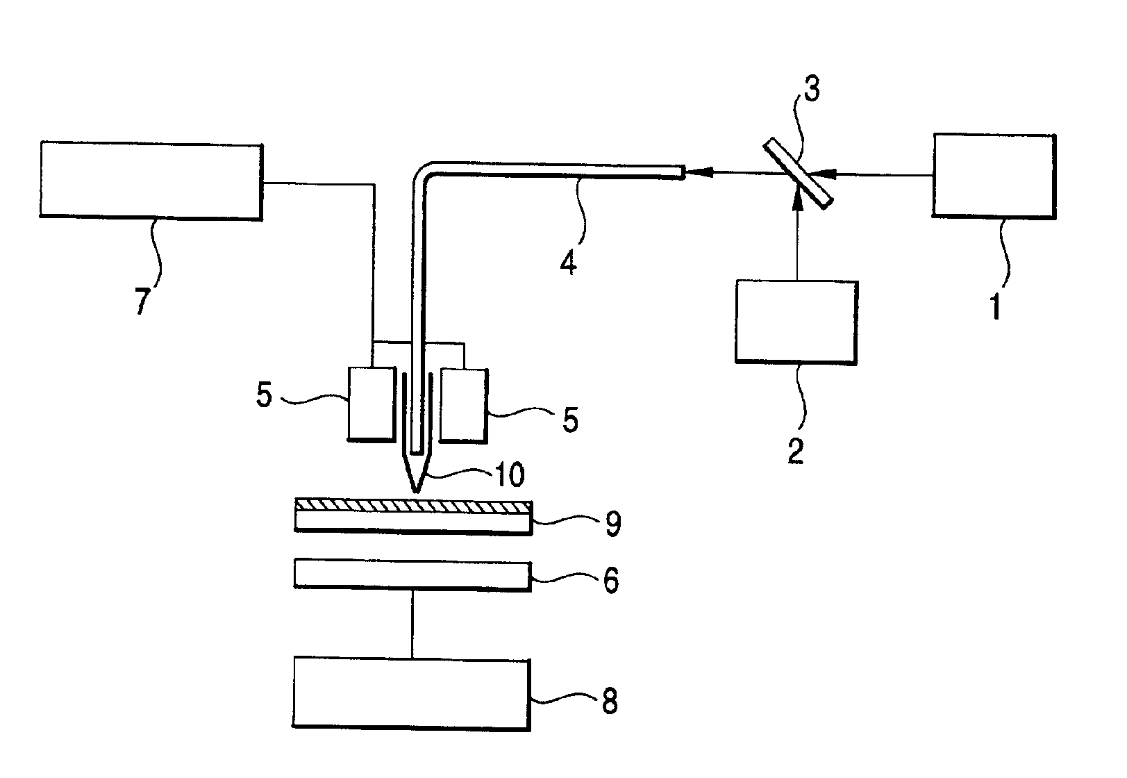
[0090]The entire surface of the recording layer was irradiated with ultraviolet light (366 nm) to make it blue. The recording medium was set on a near-field scanning optical microscope (NSOM) (TMX2100 Aurora, manufactured by Topometrix Corporation), and a beam having a wavelength of 632.8 nm from an He—Ne laser was applied to the recording layer for 1 minute. Then the entire surface w...
example 2
[0092]Compound (A) (bis(2,4-dimethyl-5-(4-t-butyl) phenylthiophen-3-yl)perfluorocyclopentene; glass transition point: 70° C.) having the formula shown below was synthesized in accordance with the process described in Preparation Example 1.
[0093]A 350 nm thick amorphous recording layer was formed on a glass substrate by using compound (A) in the same manner as in Example 1. The OD of the recording layer per 100 nm thickness was 0.65. The surface roughness (Ra) of the recording layer was 1 nm or smaller as measured with an AFM or an STM. The recording layer was totally transparent.
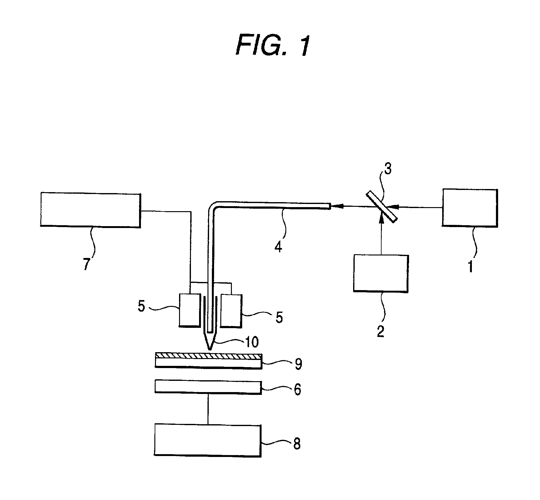
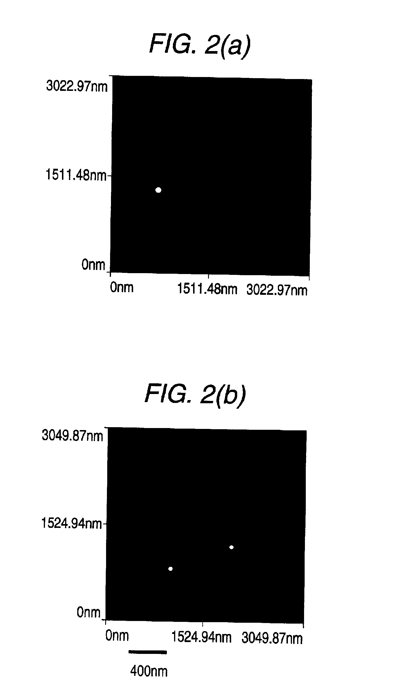
[0094]A spot was written on the recording medium, read out, and erased in the same manner as in Example 1. It was confirmed that a spot having a diameter of about 80 nm had been recorded as shown in FIG. 2A. Another spot was written on a different site and read out in the same manner. As a result, a second fine spot having a diameter of about 80 nm was recorded as shown in FIG. 2B. These recorded spots were...
PUM
 Abstract
Description
Claims
Application Information
 - R&D
- Intellectual Property
- Life Sciences
- Materials
- Tech Scout
- Unparalleled Data Quality
- Higher Quality Content
- 60% Fewer Hallucinations
Browse by: Latest US Patents, China's latest patents, Technical Efficacy Thesaurus, Application Domain, Technology Topic, Popular Technical Reports.
© 2025 PatSnap. All rights reserved.Legal|Privacy policy|Modern Slavery Act Transparency Statement|Sitemap|About US| Contact US: help@patsnap.com


