Plasma reactor having an inductive antenna coupling power through a parallel plate electrode

Inactive Publication Date: 2003-09-23
APPLIED MATERIALS INC
View PDF108 Cites 78 Cited by
  • Summary
  • Abstract
  • Description
  • Claims
  • Application Information

AI Technical Summary

Benefits of technology

It is an object of the invention to provide an induction coil antenna whose physical disposition and / or power distribution pattern is relatively uniform with reference to the entire wafer surface so that plasma ion production is not predominantly at the vicinity of the chamber side wall, while at the same time providing a uniform ground plane in close proximity to the entire wafer surface so as to avoid plasma current flow to the chamber side wall. It is a further object of the invention to employ such a ground plane in a manner that effectively confines the plasma closer to the top surface of the wafer so as to minimize interaction with the chamber side wall.
It is another object of the invention to eliminate or reduce consumable materials such as quartz or ceramics in the chamber walls, so as to avoid depletion of plasma ions near the chamber walls and consumption of expensive reactor components through etching of such materials.
It is a further object of the invention to enhance processing uniformity at the wafer center relative to the wafer periphery in such a reactor by providing a uniform etch and polymer precursor gas distribution. Specifically, it is an object of the invention to introduce such gas from an optimum radial location of the chamber, such as from the chamber center and / or from the chamber periphery, whichever optimizes process uniformity across the wafer surface. For example, where etch rate is low at the wafer center and high at the wafer periphery, the gas is preferably introduced from the center of the ceiling rather than from near the periphery of the ceiling.
It is an additional object of the invention to enhance processing uniformity at the wafer center relative to the wafer periphery in such a reactor by enhancing (or reducing, if desired) the RF induction field over the wafer center relative to the RF induction field over the wafer periphery. Specifically, it is an additional object of the invention to provide separate or independent control of the strength of the RF induction field over the wafer center and independent control of the strength of the RF induction field over the wafer periphery, so that the radial distribution of the RF induction field across the wafer surface is adjustable to optimize plasma processing uniformity across the wafer surface.
In a typical plasma processing chamber used for selective etching of thin films on a semiconductor wafer, a combination of etch and deposition processes are employed simultaneously. Polymer forms on surfaces that are either sufficiently cold (below the temperature threshold of polymerization) or on which ion bombardment is below a threshold energy (the threshold ion energy sufficient to offset the polymer deposition rate on that surface). The temperature threshold and the threshold ion energy depend upon the material of the surface. Deposition can occur on the wafer as well as the process chamber surfaces. Control of the deposition on the wafer as well as the process chamber surfaces is critical to controlling the selective etch process. Polymer deposition on interior surfaces of reactor chamber walls is required in cases where the material of the chamber walls is incompatible with the process being carried out on the wafer. One example of this is where the chamber walls are aluminum and the process being carried out is plasma etching of silicon dioxide. Deposition of polymer on the chamber wall surfaces prevents introduction of aluminum into the process by preventing plasma ion sputtering of the chamber walls.
It is therefore an additional object of the invention to eliminate the requirement to periodically clean the reactor chamber interior. It is a further object of the invention to prevent the collection of polymer on chamber surfaces in the processing region of the chamber. It is a related object to control the etch rate of those same chamber surfaces. It is a further object of the invention to provide appropriate transition from the processing region of the chamber by confining the plasma to the processing region. It is a yet further object of the invention to collect any residual polymer-forming species in areas outside the processing region of the chamber such as the pumping annulus.

Problems solved by technology

In contrast, capacitively coupled reactors typically provide relatively lower plasma ion densities (e.g., on the order of only 10.sup.10 ions / cm.sup.3) and generally cannot provide independent control of ion density and ion energy.
In contrast, parallel plate capacitively coupled plasma reactors typically stop etching at feature sizes on the order of about 0.25 microns, or at least exhibit inferior etch selectivity and etch profile due to an inferior ion-to-neutral density ratio.
However other materials such as aluminum oxide tend produce greater contamination than quartz due to sputtering.
However, the side wall is a poor ground plane, as it has many discontinuities, such as a slit valve for wafer ingress and egress, gas distribution ports or apparatus and so forth.
Such discontinuities give rise to non-uniform current distribution, which distort plasma ion distribution relative to the wafer surface.
The resulting sideways current flow toward the side wall contributes to non-uniform plasma ion distribution relative to the wafer surface.
The main problem with this type of plasma reactor is that it is liable to exhibit processing non-uniformity across the wafer surface.
The etch process near the wafer center is dependent upon such energetic electrons traveling from the vicinity of the chamber side wall and reaching the wafer center before recombining along the way by collisions with neutral species or ions, so that the etch process is not uniform across the wafer surface.
Moreover, introduction of the etchant precursor gas from the side and coupling of plasma source power from the side produces a non-uniform etchant ion / radical distribution favoring the side.
Many of the ions and radicals formed near side (over the wafer periphery) are consumed by etching the quartz side wall and are not available to etch the wafer center, while etchant ion / radical-forming energetic electrons generated near the side are lost to collisions with other species before reaching the wafer center, thus reducing the etchant ion concentration at the wafer center.
(It should be noted that the etching of the quartz side wall greatly increases the cost of operating the reactor because it consumes a very expensive item--the quartz side wall, which must be periodically replaced.)
The converse of the foregoing is that the relative plentitude of etchant ions and radicals near the wafer periphery can, under selected processing conditions, so impede polymerization as to impair etch selectivity, possibly leading to punchthrough of the underlying layer near the wafer periphery, in addition to causing a much higher etch rate at the wafer periphery.
A related problem is that the hotter electrons near the chamber side wall / wafer periphery providing more energetic plasma ions in that vicinity, coupled with the oxygen released by the etching of the quartz side wall mentioned above, erodes the edges of the photoresist mask near the wafer periphery.
Such erosion leads to faceting, in which the corners defined by the photoresist mask are etched, giving rise to an undesirable tapered etch profile.
Conversely, to avoid etch-stopping at the wafer center, the concentration of etchant ions in the plasma may be increased, which risks punchthrough or faceting near the wafer periphery.
Reducing the free fluorine concentration in this manner has the effect of not only decreasing etch rate but also enriching the carbon content of the polymer, thus increasing the effect of the polymer on the etch process to guard against punch through at the wafer periphery, but increasing the risk of etch stopping at the wafer center.
Conversely, increasing the free fluorine concentration not only increases the etch rate but also depletes the carbon content of the polymer, thus decreasing the effect of polymerization on the etch process, thus decreasing the risk of etch stopping at the wafer center but weakening the protection against punch through at the wafer periphery.
The problem with option (1) is that the polymer accumulated on the surface must be removed periodically, either by manual (wet) cleaning, by plasma (dry) cleaning, or by replacing the contaminated parts.
Otherwise, flaking of the polymer will occur, leading to contamination of the chamber.
Cleaning the reactor chamber requires the reactor operation be interrupted during the entire cleaning process, which represents a significant loss of productivity and increases the cost of operating the reactor.
Problems associated with the plasma cleaning process include not only loss of productivity but also loss of consumable materials in the chamber and contamination.
The problem with option (2) is that etching of chamber surfaces occurs because the surfaces are exposed.
For quartz surfaces, the etching can occur at such a high rate that the quartz parts must be replaced periodically at a significant cost in parts and lost production time.
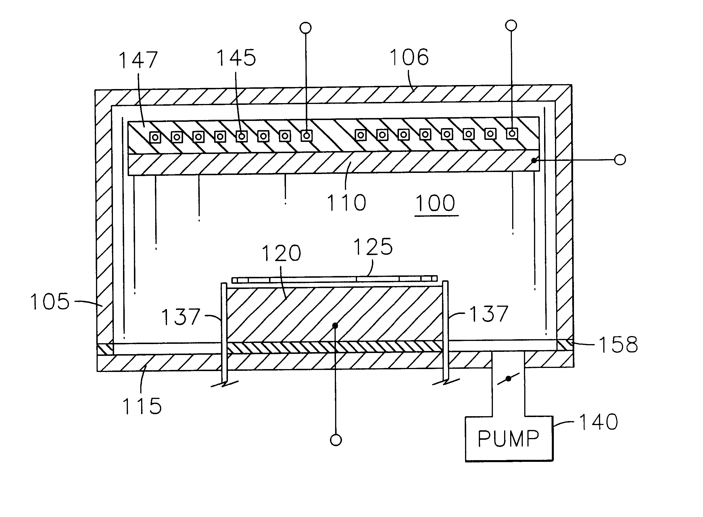
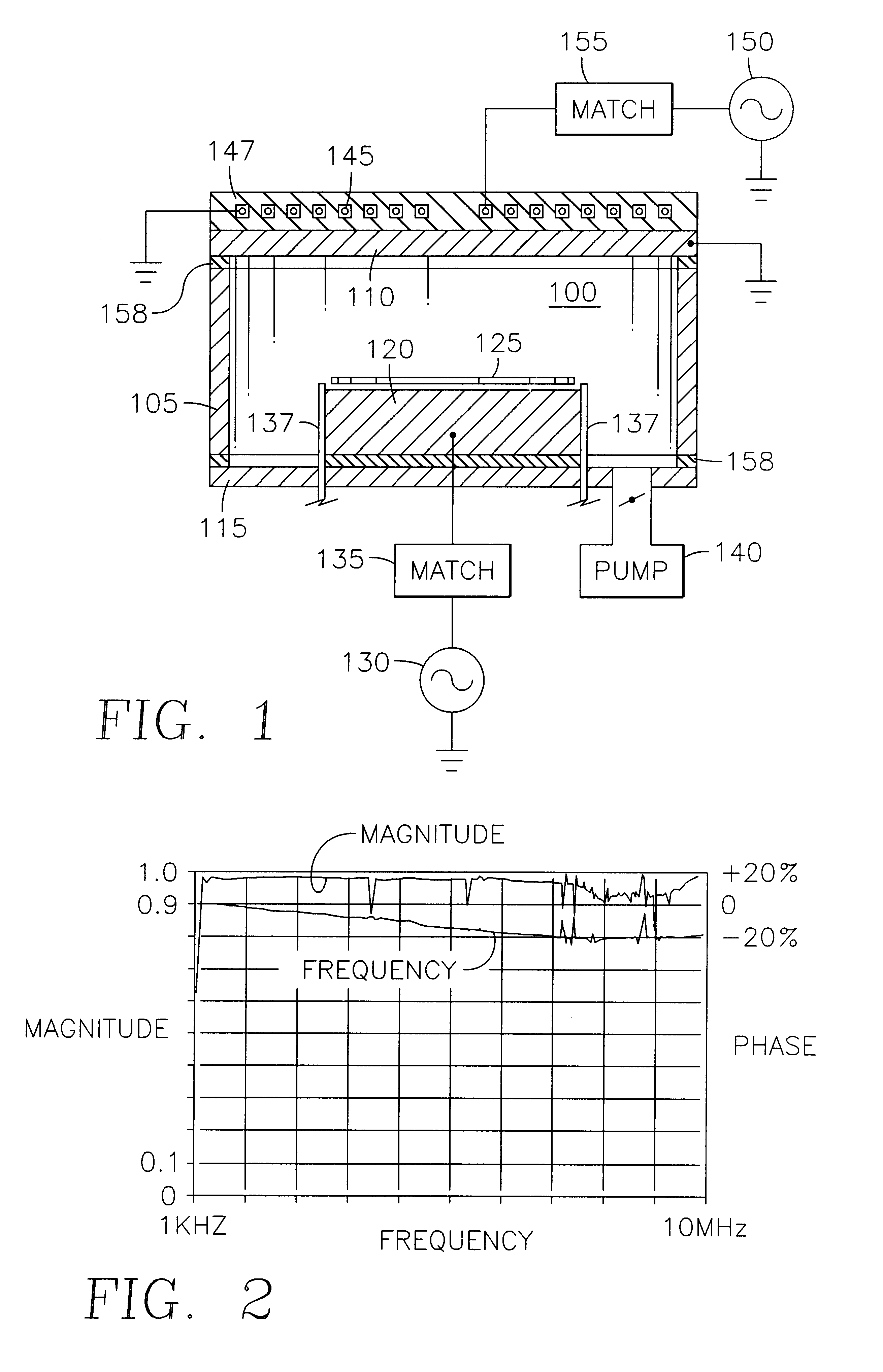
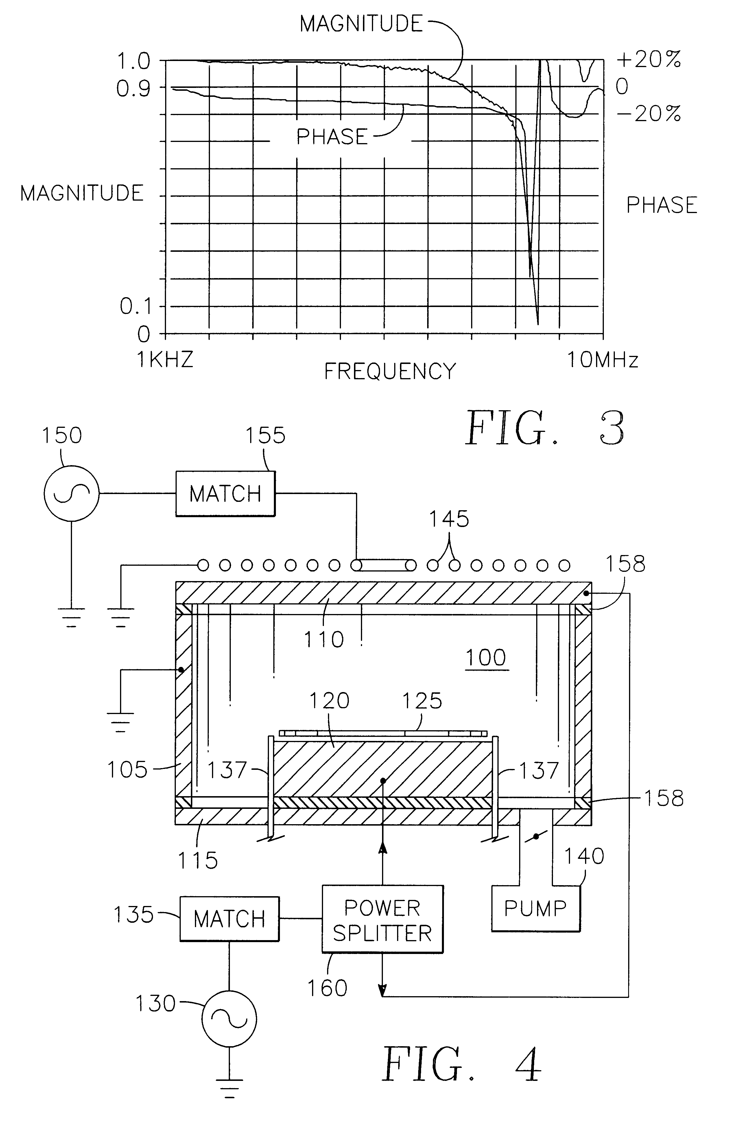
There are, however, a number of potential problems which, if not resolved, could render the reactor of FIG. 1 impractical.
First, there is the problem of whether the silicon ceiling 110 will block the RF induction field of the overhead coil antenna 145 from ever reaching the chamber 100.
Also, the RF induction field skin depth through the plasma in the chamber 100 may be greater than the chamber height (i.e., the wafer-top electrode gap), so that the RF induction power may not be efficiently coupled to the plasma.
Another problem is that the close proximity of the ceiling 110 to the wafer 125 may be insufficient to separate the plasma sheath near the ceiling 110 from the plasma sheath near the underlying wafer 125, thereby shorting out the plasma from top to bottom.
Also, insertion of the silicon material of the ceiling 110 into the RF return path of the bias RF power generator 130 may occasion significant RF bias power losses.
Finally, there may not exist a suitable or practical range of resistivity values for the semiconductor window within which an RF inductive field can be coupled without undue loss or attenuation.

Method used


Image

  • Plasma reactor having an inductive antenna coupling power through a parallel plate electrode
  • Plasma reactor having an inductive antenna coupling power through a parallel plate electrode
  • Plasma reactor having an inductive antenna coupling power through a parallel plate electrode

Examples


first embodiment

FIG. 68A illustrates a cross-sectional view of the magnetic confinement feature referred to previously in connection with the opposing magnet rings 2130, 2135 of FIG. 48A. In FIG. 68A, the magnet rings have poles which are oriented end-to-end with opposing poles facing one another. In FIG. 68B, the opposing magnet poles are oriented side-to-side in opposing directions so that opposite pair of poles are in juxtaposed alignment. In FIG. 68C, the opposing magnet poles are oriented along diagonal acute angles relative to the direction of displacement between the two magnet rings 2030, 2035. FIGS. 68D and 68E correspond to FIGS. 68B and 68C, respectively, except that like magnetic poles are juxtaposed rather than opposing magnetic poles. Other arrangements which provide the requisite diversion of ions from a straight path through the slit valve 1075 or other large opening may be provided in carrying out the invention.

While the embodiments of FIGS. 48A-68C have been described with referen...

working examples

The foregoing concepts were explored in the following working examples using a plasma reactor corresponding in general to the embodiment of FIG. 48A in which the silicon ceiling electrode 1020 had a 10-inch diameter, the cylindrical skirt 1010 had a 10-inch diameter, the gap between the wafer 1065 and the ceiling 1020 was 4 inches, the skirt 1010 was grounded and a RF bias power was applied to the wafer pedestal 1060 and to the ceiling electrode 1020. Also, RF bias power of various selected power levels at 100 kHz was applied to the ceiling 1020. Plasma source RF power of 3250 Watts at 2.0 MHz was applied to the coil 1040 and RF bias power of 1400 Watts at 1.8 MHz was applied to the wafer pedestal 1060. The chamber 1035 was held at a pressure of 50 milliTorr. The light polymer chemistry was provided by combined gas flows into the chamber 1035 of 800 sccm Argon, 100 sccm CHF.sub.3 and 38 sccm CO.sub.2. The wafer was cooled using conventional techniques to avoid overheating. In each o...


PUM

PropertyMeasurementUnit
Lengthaaaaaaaaaa
Temperatureaaaaaaaaaa
Thicknessaaaaaaaaaa

Abstract

A plasma reactor for processing a workpiece includes a reactor enclosure defining a processing chamber, a base within the chamber for supporting the workpiece during processing thereof, a semiconductor window electrode overlying the base, a gas inlet system for admitting a plasma precursor gas into the chamber, an electrical terminal coupled to the semiconductor window electrode, an inductive antenna adjacent one side of the semiconductor window electrode opposite the base for coupling power into the interior of said chamber through the semiconductor window electrode.

Description

1. Technical FieldThe invention relates to a plasma reactor having parallel plates for interposition therebetween of a workpiece to be processed, such as a semiconductor wafer, and an inductive coil antenna coupling RF power through one of the parallel plates into the interior of the reactor.2. Background ArtInductively coupled plasma reactors for processing microelectronic semiconductor wafers, such as the type of reactor disclosed in U.S. Pat. No. 4,948,458 to Ogle, enjoy important advantages over parallel-plate capacitively coupled plasma reactors. For example, inductively coupled plasma reactors achieve higher plasma ion densities (e.g., on the order of 10.sup.11 ions / cm.sup.3). Moreover, plasma ion density and plasma ion energy can be independently controlled in an inductively coupled plasma reactor by applying bias power to the workpiece or wafer. In contrast, capacitively coupled reactors typically provide relatively lower plasma ion densities (e.g., on the order of only 10.s...

Claims


Application Information

Patent Timeline
IPC IPC(8): A23G3/34A23G9/52A23L1/05A23L1/0524A23L1/052A23L1/0532A23L1/054A23L1/0526A23L1/187A23L1/214A23L1/236A23L2/52A21D2/00A21D2/18A23L1/308A23L2/60H01L21/683H01L21/67H01J37/32H05H1/46A23L9/10A23L19/10A23L27/30A23L29/231A23L29/238A23L29/256A23L29/269H01L21/302H01L21/3065
CPCA21D2/185A23G3/346A23G9/52A23L1/0524A23L1/0526A23L1/0532A23L1/0541A23L1/1875A23L1/2147A23L1/236A23L1/2362A23L1/308A23L2/60H01J37/321H01J37/32165H01J37/32458H01J37/32467H01J37/32522H01J37/32871H01L21/6831A23G2200/06H01J2237/3345H01J2237/3346A23L9/12A23L19/115A23L27/30A23L27/32A23L29/231A23L29/238A23L29/256A23L29/27A23L33/21
Inventor COLLINS, KENNETH S.RICE, MICHAELTROW, JOHNBUCHBERGER, DOUGLASASKARINAM, ERICTSUI, JOSHUA CHIU-WINGGROECHEL, DAVID W.HUNG, RAYMOND
Owner APPLIED MATERIALS INC
Why Eureka
Try Eureka