Eureka AIR delivers breakthrough ideas for toughest innovation challenges, trusted by R&D personnel around the world.

Semiconductor device and manufacturing method therefor

Inactive Publication Date: 2003-02-04
KK TOSHIBA
View PDF12 Cites 80 Cited by
  • Summary
  • Abstract
  • Description
  • Claims
  • Application Information

AI Technical Summary

Benefits of technology

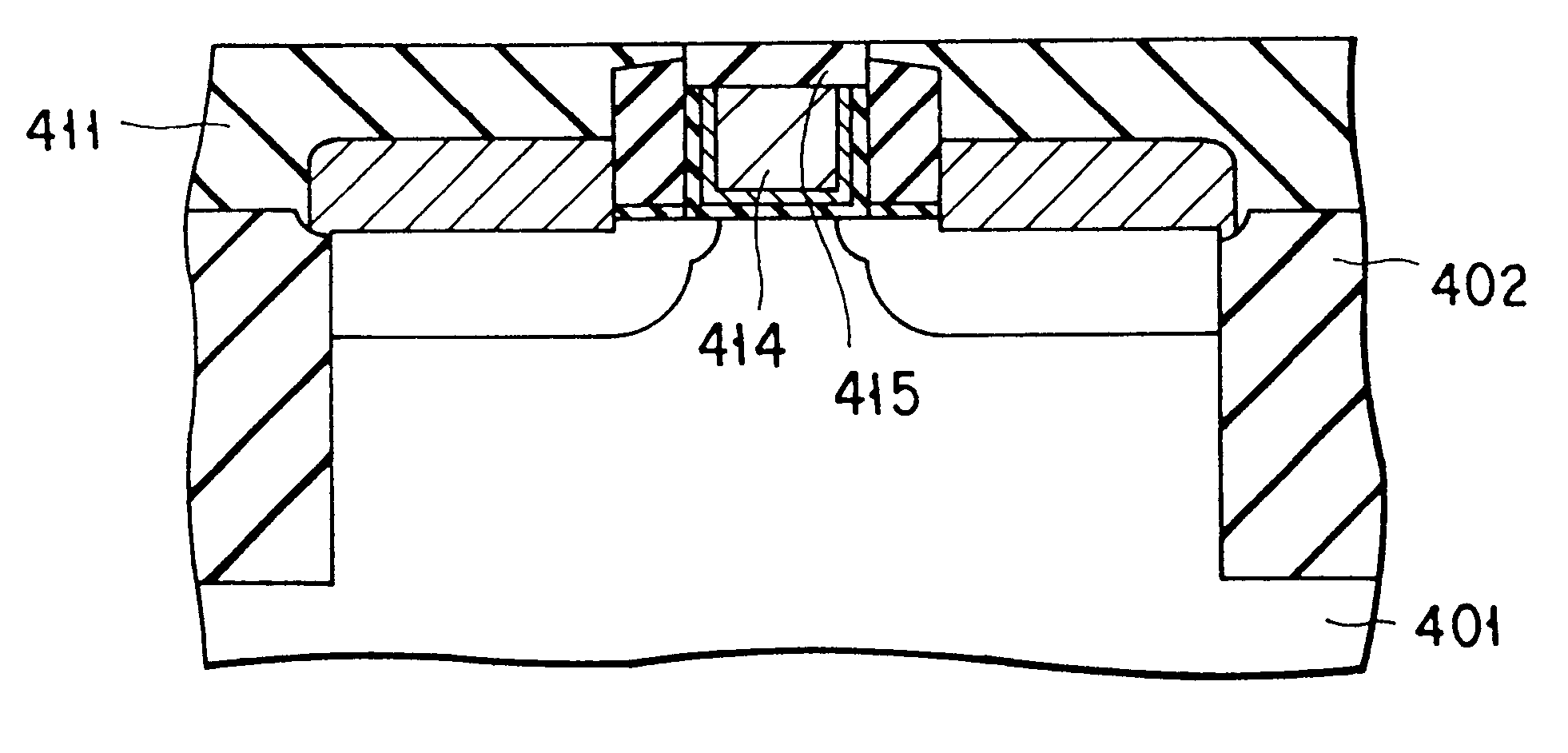
Accordingly, it is a primary object of the present invention to provide a manufacturing method for a semiconductor device which can suppress local concentration of an electric field on edge corner portions of a device region, thereby preventing deterioration of the characteristic of a transistor.
It is another object of this invention to provide a manufacturing method for a semiconductor device which has a wider margin against a variation at the time of forming a side wall on the side wall of a gate electrode to thereby ensure manufacturing of semiconductor devices with a high yield.
It is a different object of this invention to provide a manufacturing method for a semiconductor device which prevents a groove from becoming wider at the time of removing a dummy gate layer to thereby ensure manufacturing of fine semiconductor devices.
It is a further object of this invention to provide a manufacturing method for a semiconductor device which can fabricate fine semiconductor devices without increasing the parasitic capacitance of each device.
It is still further object of this invention to provide a semiconductor device whose gate electrode has a reduced resistance and in which a step formed by the gate electrode is suppressed.

Problems solved by technology

The miniaturization of devices, which can be accomplished by using the STI (Shallow Trench Isolation) technique, faces a problem of an increased wiring resistance.
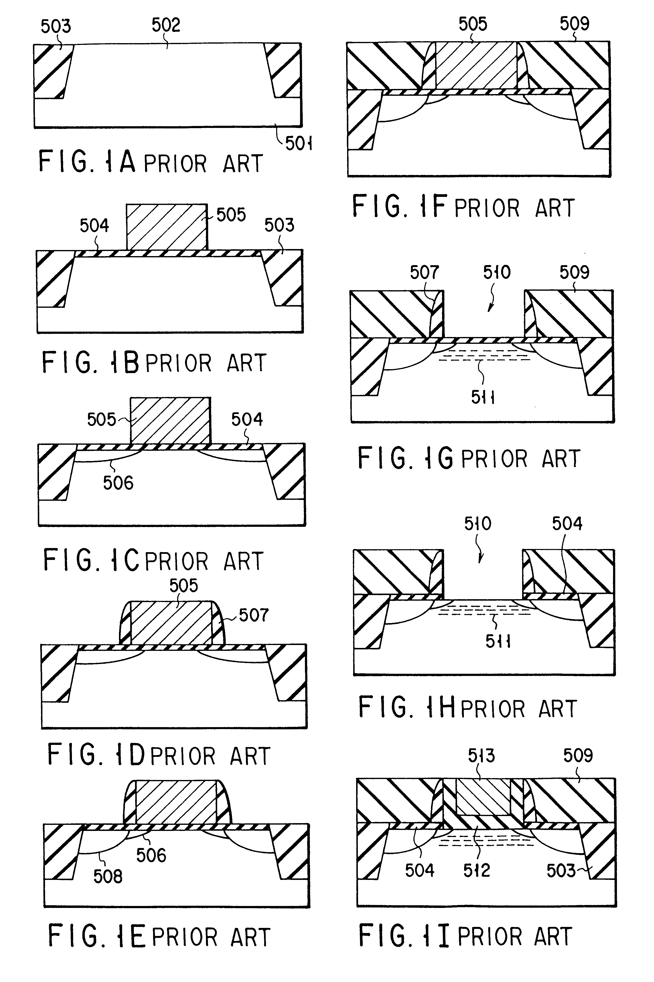
In a conventional case where a source / drain region is formed after forming a gate insulator film and a gate electrode, a high temperature treatment and thermal oxididation are required, which raise such problems as the increased resistance of the metal electrode and deterioration of the reliability of the gate insulator film.
As a result, an electric field is concentrated on the edge corners, resulting in deterioration of the transistor characteristics, such as a lower reliability of the gate insulator film.
In the conventional transistor manufacturing method which forms a source / drain region using a dummy gate pattern and then forming a gate insulator film and a gate electrode in a groove formed by removing the dummy gate pattern, large dents are formed at the edge corners of the isolation region, exposing the edge corners of the device region, so that an electric field is concentrated on the edge corners, deteriorating the transistor characteristics.
In the case of ordinary transistors, when a silicon nitride film is used as an etching stopper to be formed on the gate electrode and the sidewall insulator film 507 of the gate electrode, the parasitic capacitance may not become low enough to meet the requirements of ultra-miniaturization and fast operation because the dielectric constant of the silicon nitride film is not so low.
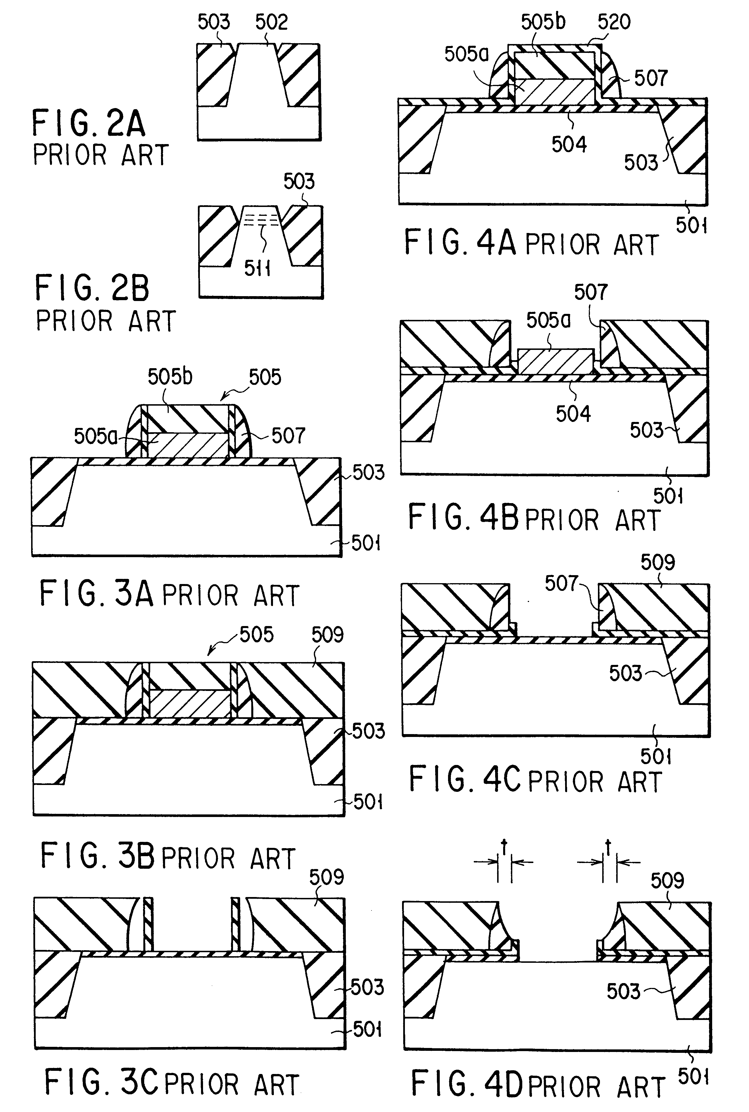
The above-described prior art however sets the size of actual completed transistors wider than the designed width of the dummy gate, which is disadvantageous for device miniaturization.
This is disadvantageous in implementing a high-frequency operation in consideration of the interline capacitance.
The wider transistor size also reduces a margin for patterning the interlayer insulator film for forming contacts in the source and drain regions, so that the minimum design size should be set larger accordingly, which is also disadvantageous in implementing a higher integration density.
This cannot ensure a sufficient gate height; in a case where the dummy gate is comprised of a polycrystalline film of 200 nm in thickness and a silicon nitride film of 200 nm in thickness, for example, the gate height after the formation of the gate becomes very low. consequently, the resistance of the gate line becomes higher, resulting in increased dissipation power and impaired dielectric characteristic.
Because this process cannot employ a so-called LDD structure which has a lighter impurity concentration of the diffusion layer at the gate's edge portions at a shallower depth, it is difficult to suppress a short channel effect.
As the recent device miniaturization progresses to fabricate transistors with a gate length of 0.1 .mu.m or shorter, however, the parasitic resistance of the polycrystalline silicon gate electrode becomes too large to be neglected, deteriorating the device performance.
This makes it difficult to form ultra-small gates.
The new use of a material having such a property in the semiconductor manufacturing process involves significant difficulty.
Making the gate oxide film thinner than the level at which direct tunneling occurs (e.g., a thickness smaller than about 3 nm) is considered inappropriate from the viewpoint of the reliability of transistors.
The conventional polycide gate structure (the lamination of a polysilicon film and a silicide film), as the width of the gate electrode becomes narrower, the thickness of the gate electrode becomes thicker, undesirably increasing the steps of the gate electrode.
However, the metal gate electrode is not a good choice in view of the heat resistivity.
It is however difficult for the gate insulator film (high-dielectric film) to endure such a high-temperature treatment.
This results in deterioration of the gate insulator film, making it difficult to provide MOS transistors with good electric characteristics.
As it is difficult to remove such an etching damage, the device characteristics will not be improved as expected.
In the conventional MOS transistor with a groove channel structure, as apparent from the above, the gate electrode extends over the source / drain diffusion layer, it is necessary to put some distance between the gate electrode and the source / drain line electrode, which makes ultra-miniaturization of devices difficult.
This raises such a problem that the aspect ratio of a contact hole becomes larger at the time of forming the contact hole in the gate electrode.

Method used


Image

  • Semiconductor device and manufacturing method therefor
  • Semiconductor device and manufacturing method therefor
  • Semiconductor device and manufacturing method therefor

Examples


first embodiment

FIGS. 9A through 9I and FIGS. 10A through 10I are cross-sectional views showing a manufacturing process for a semiconductor device according to the first embodiment of the invention. FIGS. 9A-9I illustrate the cross-section of a transistor in a gate length direction, and FIGS. 10A-10I illustrate the cross-section of the transistor in a gate width direction.

First, an SiO.sub.2 film 102 about 10 nm thick is formed on the surface of an Si substrate 101 by thermal oxidization or the like. Then, an amorphous Si film 103 and Si.sub.3 N.sub.4 film 104 about 200 nm and 100 nm thick, respectively, are deposited on the SiO.sub.2 film 102 by LPCVD. The amorphous Si film 103 may contain a donor such as phosphorus or arsenic (FIGS. 9A and 10A).

Next, the SiO.sub.2 film, amorphous Si film 103 and Si.sub.3 N.sub.4 film 104 are processed into an island-like pattern by, for example, lithography or RIE (FIGS. 9B and 10B).

Then, the Si substrate 101 is etched by RIE, self-aligned with the previously for...

second embodiment

A first example of the second embodiment will now be described with reference to FIGS. 11A through 11H, 12 and 13. FIGS. 11A-11H are cross-sectional views in the gate length direction (the cross section along line 11--11 in FIG. 13), showing a manufacturing process for a semiconductor device according to this specific example. FIG. 12 is a cross-sectional view in the gate width direction (the cross section along the line 12--12 in FIG. 13) and corresponds to FIG. 11H.

First, an amorphous silicon film 203, which will be a dummy gate pattern, is deposited 100 nm thick on a buffer oxide film 202, which has been formed on a silicon substrate 201 (FIG. 11A).

Next, a resist pattern (not shown) for forming a device region is formed. With the resist pattern used as a mask, the amorphous silicon film 203, buffer oxide film 202 and silicon substrate 201 are etched by RIE, forming lands 204 to be device regions and making a groove 205 to be an isolation region (FIG. 11B).

Next, a buried insulator...

third embodiment

A first example of the third embodiment will now be described with reference to FIGS. 25A through 25H, 26 and 27. FIGS. 25A-25H are cross-sectional views in the gate length direction (the cross section along the line 25--25 in FIG. 27), showing a manufacturing process for a semiconductor device according to this specific example. FIG. 26 is a cross-sectional view in the gate width direction (the cross section along the line 26--26 in FIG. 27) and corresponds to FIG. 25H.

First, a silicon film 303 of polycrystalline silicon or amorphous silicon, which contains an impurity and which is to be part of a gate line, is deposited 100 nm thick on a gate insulator film 302 formed on a silicon substrate 301. Note that an impurity is implanted into-the substrate, as needed, to control the substrate concentration, before the deposition of the gate electrode (FIG. 25A).

Next, a resist pattern (not shown) for forming a device region is formed. With the resist pattern used as a mask, the silicon fil...


PUM


Abstract

A method of manufacturing semiconductor device comprises the steps of forming a first film and a second film on a semiconductor substrate, selectively removing the second film, the first film and a top portion of the semiconductor substrate to form a first groove, burying a first insulator film in the first groove to form an isolation region, patterning the second film surrounded by the isolation region to form a dummy gate layer, doping the semiconductor substrate with an impurity using the dummy gate layer as a mask, forming a second insulator film on the semiconductor substrate surrounded by the dummy gate layer and the first insulator film, removing the dummy gate layer and the first film to form a second groove, forming a gate insulator film on the semiconductor substrate in the second groove, and forming a gate electrode on the gate insulator film in the second groove.

Description

BACKGROUND OF THE INVENTIONThe present invention relates to a semiconductor device and a manufacturing method thereof, and, more particularly, to a manufacturing method of manufacturing a semiconductor device which includes a step of forming a dummy gate.To implement a higher performance and lower cost of a semiconductor integrated circuit using MOS transistors, miniaturization of devices is important. The miniaturization of devices, which can be accomplished by using the STI (Shallow Trench Isolation) technique, faces a problem of an increased wiring resistance. To overcome this problem, a scheme of reducing the wiring resistance using a metal material of a low resistance for the gate electrode has been proposed.In a conventional case where a source / drain region is formed after forming a gate insulator film and a gate electrode, a high temperature treatment and thermal oxididation are required, which raise such problems as the increased resistance of the metal electrode and deterio...

Claims


Application Information

Patent Timeline
IPC IPC(8): H01L21/28H01L21/70H01L21/336H01L21/60H01L21/768H01L29/40H01L21/8234H01L21/02H01L29/49H01L29/423
CPCH01L21/28114H01L21/76801H01L21/76829H01L21/76831H01L21/76832H01L21/76834H01L21/76897H01L21/823437H01L29/41783H01L29/495H01L29/6653H01L29/66545H01L29/6659H01L29/66621H01L29/78H01L21/28123Y10S257/90H01L29/4941H01L29/66537
Inventor INUMIYA, SEIJISAITO, TOMOHIROYAGISHITA, ATSUSHIHIEDA, KATSUHIKOIINUMA, TOSHIHIKO
Owner KK TOSHIBA
Why Eureka
Eureka Blog
Learn More