High Dynamic Range Single Photon Avalanche Detector Array on Silicon with Circuitry for Light Detection and Ranging

Pending Publication Date: 2021-11-04
SEMIKING LLC
View PDF0 Cites 1 Cited by
  • Summary
  • Abstract
  • Description
  • Claims
  • Application Information

AI Technical Summary

Benefits of technology

The patent describes a method for making a special type of image sensor called a SPAD device. The method involves depositing a thin screen oxide on a clean, defect-free surface and then using ion implantation and annealing to create doped regions in the sensor. The resulting device has a high sensitivity and low dark count rate. The patent also discusses the use of a thin screen oxide to protect the sensor from contamination during the process. The sensor can be combined with other components to create a small pixel size and a low cost for use in automotive applications. The sensor includes a single SPAD in each pixel, a quench transistor, and a CMOS inverter element to provide an input pulse to a time-to-analog converter. The sensor can be used in a two-dimensional array with a smaller pixel pitch.

Problems solved by technology

This ability to focus poses an inherent danger to human sight if the laser illumination levels used in the LiDAR system exceed the maximum permissible exposure (MPE).
The resultant hybrid image sensor formed by this bonding process exhibits problems with reliability, semiconductor manufacturing yield, chip size, and most importantly high cost.
The size of the indium bump itself limits pixel dimensions thus electronic innovations accomplished in related fields such as CMOS scaling cannot be used to their fullest extent.
However, germanium has a 4 percent lattice mismatch to silicon rendering a highly defective layer when epitaxially grown directly on silicon.
Minority carrier p-n junction devices fabricated in this Ge material possess very high dark current and thus high noise.
The high noise of these devices makes them useless for high performance LiDAR and for photon starved applications like low light imaging.
A simple photodetector using these nearly defect-free semiconductor regions yields low dark current, but does not have enough sensitivity for long range LiDAR applications.

Method used


Image

  • High Dynamic Range Single Photon Avalanche Detector Array on Silicon with Circuitry for Light Detection and Ranging
  • High Dynamic Range Single Photon Avalanche Detector Array on Silicon with Circuitry for Light Detection and Ranging
  • High Dynamic Range Single Photon Avalanche Detector Array on Silicon with Circuitry for Light Detection and Ranging

Examples


Embodiment Construction

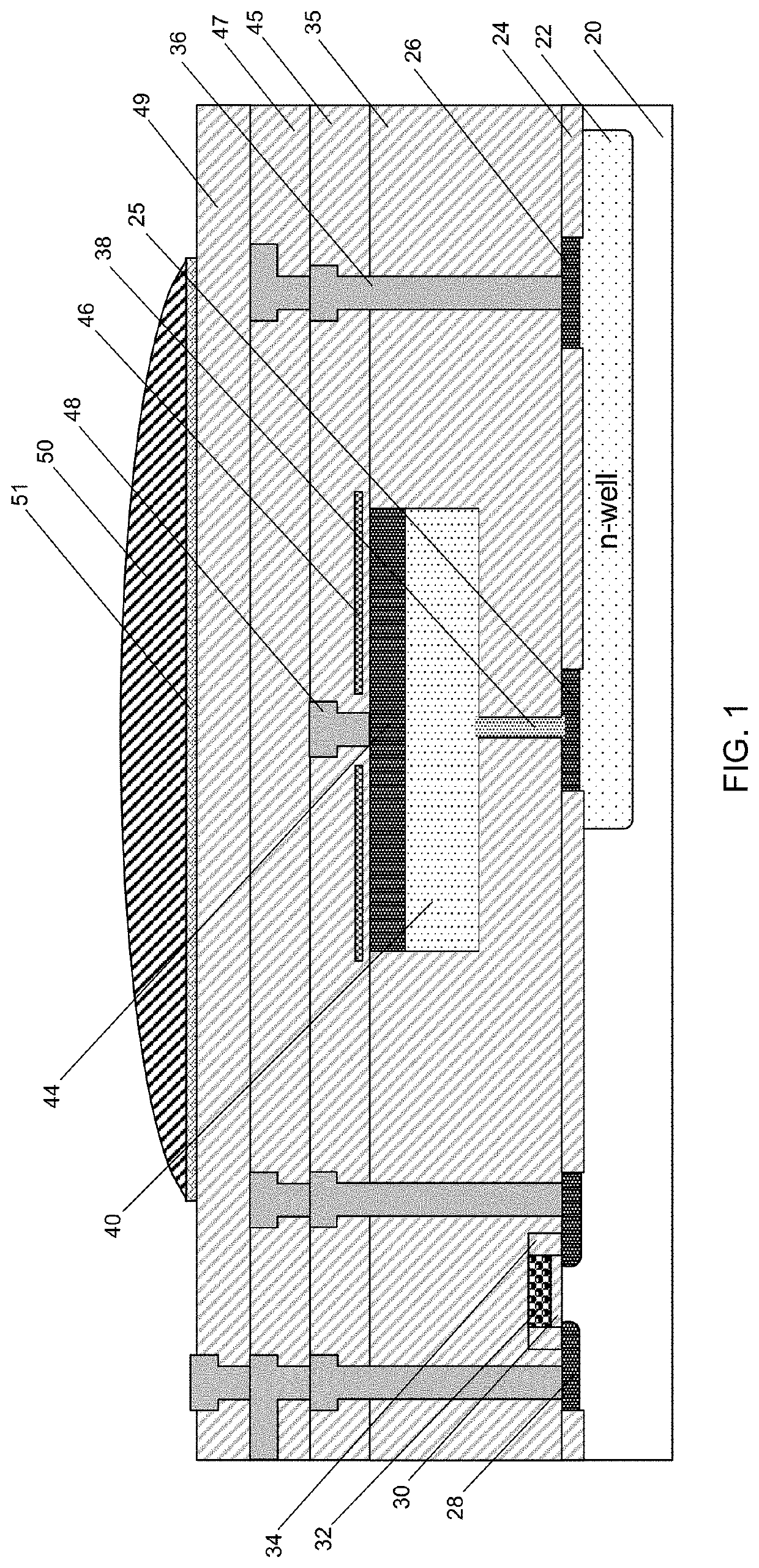
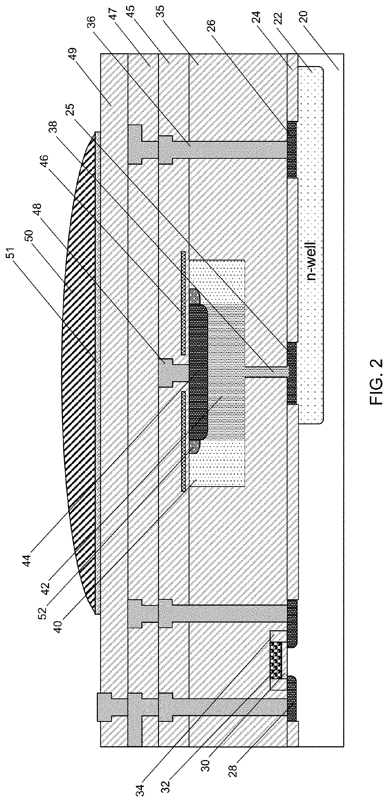
[0012]The fabrication of a germanium single photon avalanche detector (SPAD) array begins with a conventional silicon complementary metal oxide semiconductor (CMOS) process and is interrupted after the formation of the first metal via. Nearly defect free germanium isolated regions are formed through selective epitaxial growth and chemical mechanical polishing on the CMOS silicon wafer.

[0013]The SPAD is made with CMOS compatible steps including selective epitaxial growth, ion implantation, and low temperature dielectric deposition. The high aspect ratio seed trench is formed on an n-well region formed in the substrate and serves as the cathode contact to the SPAD. The Ge seed epitaxial growth is in-situ doped with phosphorous to ensure electrical continuity to the n-well region. The n-well region extends within the substrate underneath the Ge region allowing it to be contacted with an n+ source / drain region and backend metallization as conventionally achieved to CMOS transistors.

[001...


PUM


Abstract

An image sensor array includes a substrate and a plurality of pixels. Each pixel includes a single photon avalanche detector (SPAD), a quench device coupled to a respective SPAD and configured to quench an avalanche current, and time measurement circuitry configured to measure a time-of-flight of a photon. The SPAD has a trench coupled to the substrate and having a lattice mismatch with the substrate, and a substantially defect-free region coupled to the trench and configured to generate the avalanche current when the photon is detected in the defect-free region, wherein the trench and the defect-free region form an electrode. An imaging system includes an infrared laser configured to provide a pulse of light, and the image sensor array configured to receive the pulse from the infrared laser.

Description

CROSS REFERENCE TO RELATED APPLICATIONS[0001]The present application claims the benefit of U.S. Provisional Patent Application No. 63 / 017,292 filed Apr. 29, 2020, U.S. Provisional Patent Application No. 63 / 033,315 filed Jun. 2, 2020, and U.S. Provisional Patent Application No. 63 / 117,631 filed Nov. 24, 2020, the disclosures of which are incorporated by reference herein in their entirety.BACKGROUND OF THE INVENTIONField of the Invention[0002]This invention relates to a single photon avalanche detector array fabricated on a silicon wafer with circuitry to form a receiver for a light detection and ranging system or medical imaging system that is sensitive to radiation in the visible to shortwave infrared spectral region.Discussion of the Related Art[0003]Image sensors capable of creating images in the infrared spectral region, especially shortwave infrared (SWIR), are important in a wide variety of applications including fiber optic communications, light detection and ranging (LiDAR), ...

Claims


Application Information

Patent Timeline
IPC IPC(8): G01S17/894G01S7/4863H04N5/33
CPCG01S17/894H04N5/33G01S7/4863H01L31/02027G01S17/10H01L27/14612H01L27/14636H01L27/14625H01L31/02327H01L31/1892H01L31/107
Inventor KING, CLIFFORD ALANABERG, ANDERS INGVAR
Owner SEMIKING LLC
Why Eureka
Try Eureka