Dielectric film and dielectric element

a dielectric element and dielectric film technology, applied in the direction of fixed capacitors, thin/thick film capacitors, metallic material coating processes, etc., can solve the problems of difficult to achieve the currently required capacitance, no consideration, and difficulty in solving the problem, so as to achieve maximum two-layer characteristics, increase grain boundary resistivity, and high dielectric constant

Active Publication Date: 2016-11-10
TDK CORPARATION
View PDF6 Cites 3 Cited by
  • Summary
  • Abstract
  • Description
  • Claims
  • Application Information

AI Technical Summary

Benefits of technology

The present invention provides a dielectric film with a small difference in dielectric constant between with and without the direct-current voltage applied and a high dielectric constant even with the direct-current voltage applied. The invention achieves this by controlling the resistivity of the crystal grains at the grain boundaries through the use of a sub-component containing at least one of divalent metal elements and trivalent metal elements. This results in a layer with higher resistivity containing spherical crystal grains with many grain boundaries, which can be controlled by allowing the main component to contain the sub-component of the present invention. A dielectric element is also provided.

Problems solved by technology

However, when the laminated ceramic capacitor is embedded in an electric circuit board, the thickness of the laminated ceramic capacitor and brittleness due to a ceramic property cause the problem of producing, by the stress generated in an embedding process, cracks in the laminated ceramic capacitor or deformation in a portion of the electric circuit board where the laminated ceramic capacitor is embedded.
It is difficult to resolve the problem even by a usual laminated ceramic capacitor having a very small shape.
However, the dielectric constant is as low as about 450, and thus it is difficult to achieve the currently required capacitance.
In addition, no consideration is given to the behaviors of the dielectric constant with direct-current voltage, and no description is made of knowledge about changes in the dielectric constant or capacitance with the structure and direct-current voltage.
In many cases, multilayering cannot be performed because of thicknesses.
On the other hand, when thinning of a dielectric film is performed, as an adverse effect, a high voltage is applied to the thinner dielectric film during use, and thus a higher field intensity than usual is applied to the dielectric film.
This causes the problem of decreasing the dielectric constant of the dielectric film, resulting in decrease in the capacitance of a dielectric element.

Method used


Image

  • Dielectric film and dielectric element
  • Dielectric film and dielectric element

Examples


example 1 , examples 3 to 31

Example 1, Examples 3 to 31, and Comparative Examples 3 to 13

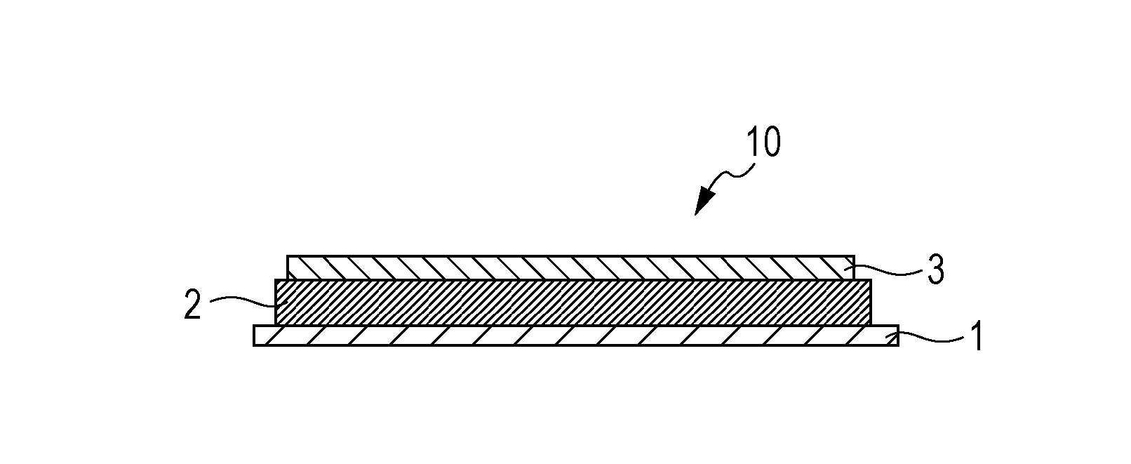
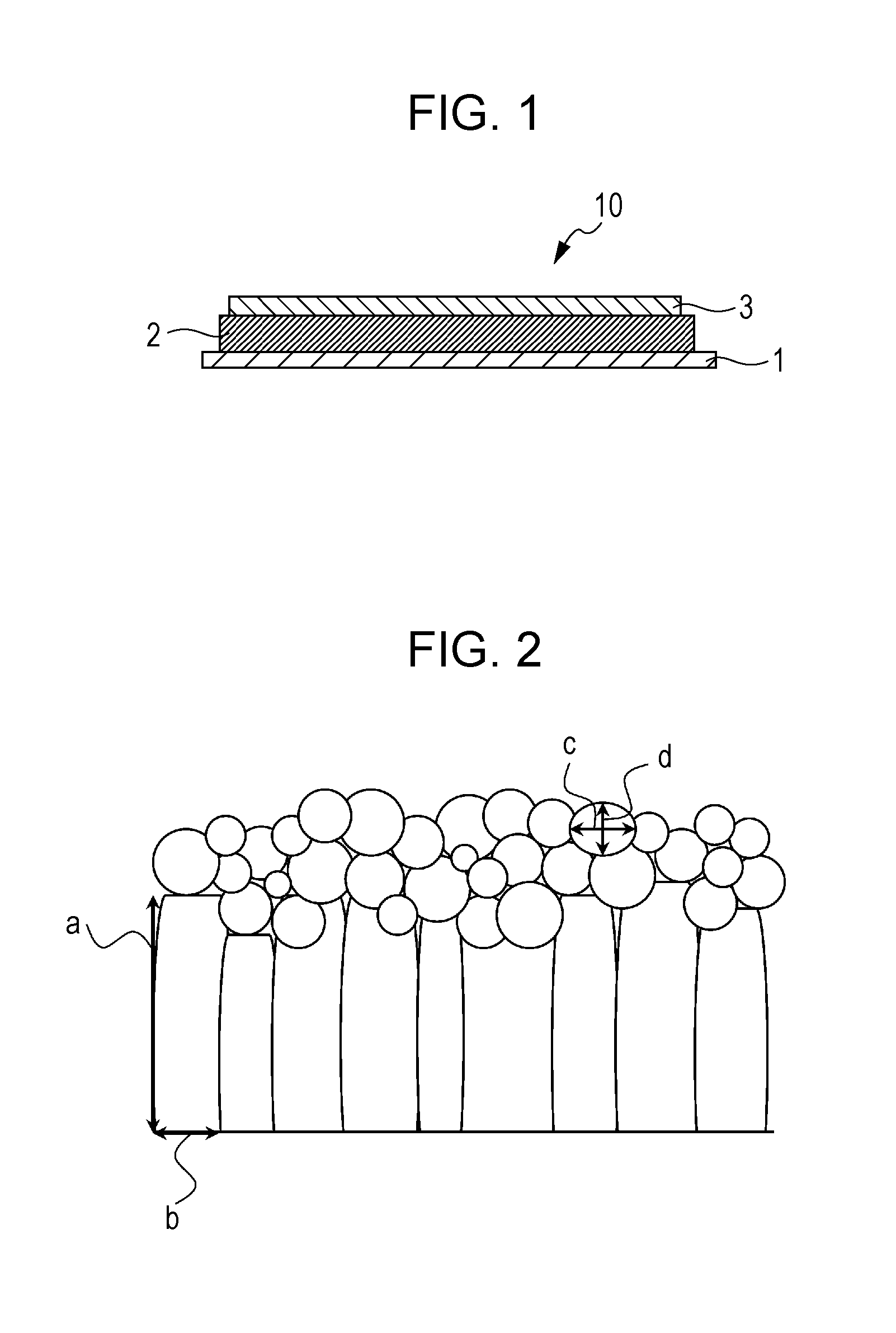
[0055]A Ni plate having a thickness of 50 μm was prepared as a lower electrode. The Ni plate had dimensions of 10 mm in length and 10 mm in width.

[0056]A target for sputtering was produced by a solid phase method. The mixing ratios of raw material powders of BaO, CaO, SrO, TiO2, and ZrO2 in the target and a sub-component were adjusted so as to obtain each of the dielectric film compositions shown in Table 1 to Table 4.

[0057]Next, the raw material powders were wet-mixed in a ball mill for 20 hours using water as a solvent, and the resultant mixed powder was dried at 100° C.

[0058]The mixed powder was pressed to form a molded body. The molding conditions included a pressure of 100 Pa, a temperature of 25° C., and a pressing time of 3 minutes.

[0059]Then, the molded body was sintered at a retention temperature of 1300° C. for a temperature keeping time of 10 hours in an air atmosphere.

[0060]Then, the resultant sintered body was...

example 32

[0087]A target for sputtering was produced by the same solid-phase method as in Example 1. The mixing ratios of raw material powders of BaO, CaO, TiO2, and ZrO2 in the target and a sub-component were adjusted so as to obtain the dielectric film composition shown in Table 5.

[0088]A dielectric film was formed under the same conditions as in Example 1.

[0089]Annealing was performed under annealing conditions including a (wet N2+H2) mixed gas atmosphere (oxygen partial pressure of 3×10⁻¹¹ MPa), a heating rate of 600° C. / hour, a retention temperature of 950° C., a retention time of 1.0 hour.

[0090]Then, a sample of Example 32 was formed by the same method as in Example 1 except that the annealing conditions were as described above.

[0091]The resultant sample of Example 32 was evaluated by the same method as in Example 1. The results are shown in Table 5.

example 33

[0092]A target for sputtering was produced by the same solid-phase method as in Example 1. The mixing ratios of raw material powders of BaO, CaO, TiO2, and ZrO2 in the target and a sub-component were adjusted so as to obtain the dielectric film composition shown in Table 5.

[0093]A dielectric film was formed under the same conditions as in Example 1.

[0094]Annealing was performed under annealing conditions including a (wet N2+H2) mixed gas atmosphere (oxygen partial pressure of 3×10⁻¹¹ MPa), a heating rate of 600° C. / hour, a retention temperature of 950° C., a retention time of 1.0 hour. Then, annealing was performed under annealing conditions including a (wet N2+H2) mixed gas atmosphere (oxygen partial pressure of 1×10⁻⁶ MPa), a heating rate of 600° C. / hour, a retention temperature of 500° C., a retention time of 1.0 hour.

[0095]A sample of Example 33 was formed by the same method as in Example 1 except that the annealing conditions were as described above.

[0096]The resultant sample o...


PUM

PropertyMeasurementUnit
dielectric constantaaaaaaaaaa
thicknessaaaaaaaaaa
thicknessaaaaaaaaaa

Abstract

The present invention relates to a dielectric element such as a thin-film capacitor including a dielectric film. The dielectric film contains a main component represented by the general formula (Ba1-xCax)z(Ti1-yZry)O3 wherein 0<x≦0.500, 0<y≦0.350, and 0.900≦z≦0.995. The dielectric film includes a layer containing columnar crystal grains and a layer containing spherical crystal grains, and contains as a sub-component at least one of divalent metal elements and trivalent metal elements.

Description

BACKGROUND OF THE INVENTION[0001]1. Field of the Invention[0002]The present invention relates to a dielectric film and a dielectric element such as a thin-film capacitor which includes the dielectric film.[0003]2. Description of the Related Art[0004]With multi-functionalization of electronic apparatuses, various functions are desired to be added to electronic circuit boards contained in electronic apparatuses. Therefore, the number of electronic components mounted on an electronic circuit board tends to increase. Thus, there is strong demand for improving the mounting density of electronic components.[0005]One of the proposed answers to the demand is to embed electronic components in an electric circuit board. One of the many electronic components mounted on an electronic circuit board is a usual laminated ceramic capacitor. However, when the laminated ceramic capacitor is embedded in an electric circuit board, the thickness of the laminated ceramic capacitor and brittleness due to ...

Claims


Application Information

Patent Timeline
Patent Type & Authority Applications(United States)
IPC IPC(8): H01G4/33H01G4/12
CPCH01G4/33H01G4/1245H01G4/1227C04B35/4682C04B35/62218C04B35/6261C04B2235/3208C04B2235/3217C04B2235/3224C04B2235/3241C04B2235/3244C04B2235/3262C04B2235/3281C04B2235/3286C04B2235/604C04B2235/6567C04B2235/787C04B2235/788C04B2235/79C23C14/088H01G4/085
Inventor TAKEDA, SAORIFURUKAWA, MASAHITOKOSUDA, MASANORIOOTSUKI, SHIROUHARADA, YASUNORI
Owner TDK CORPARATION
Why Eureka
Try Eureka