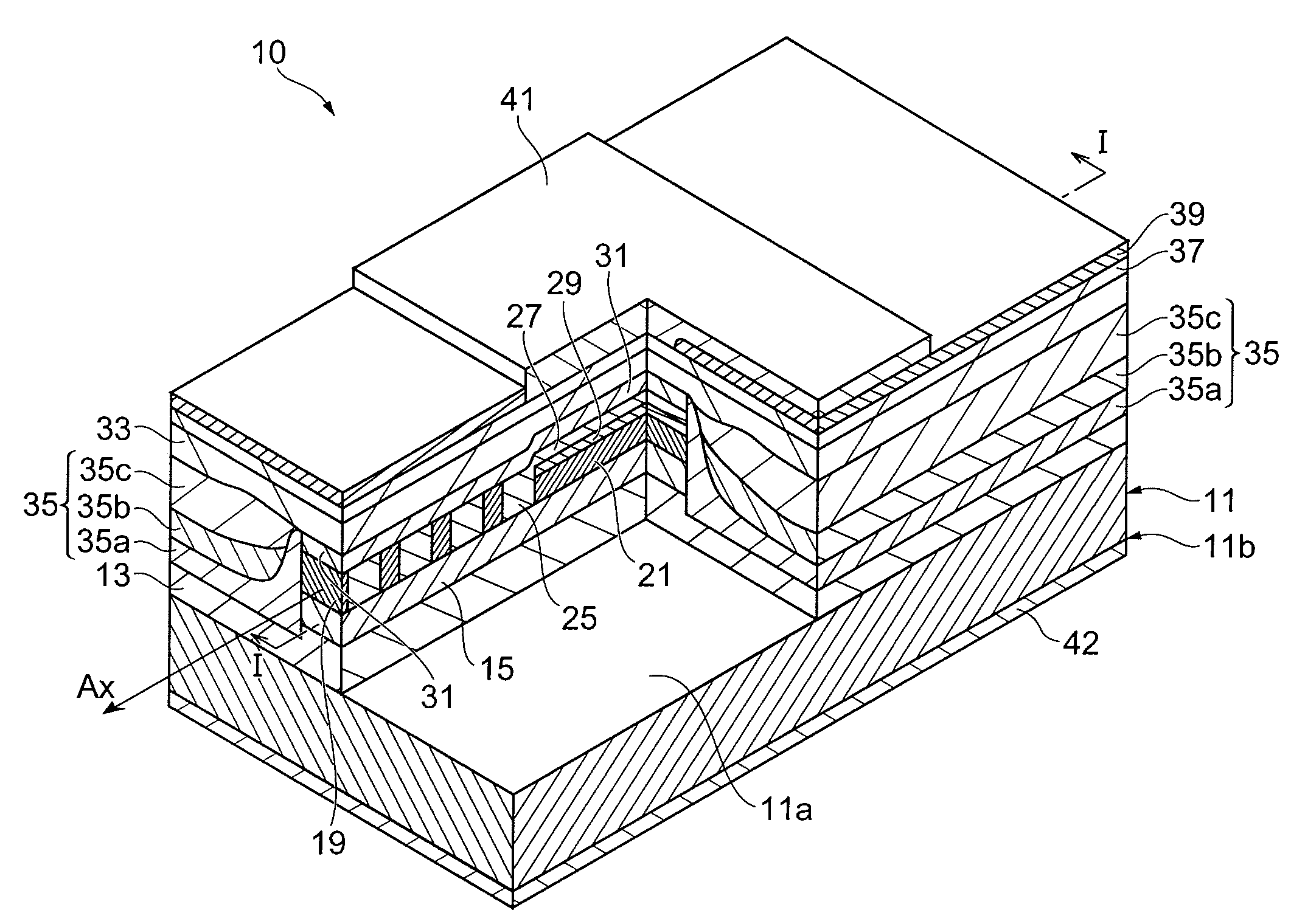
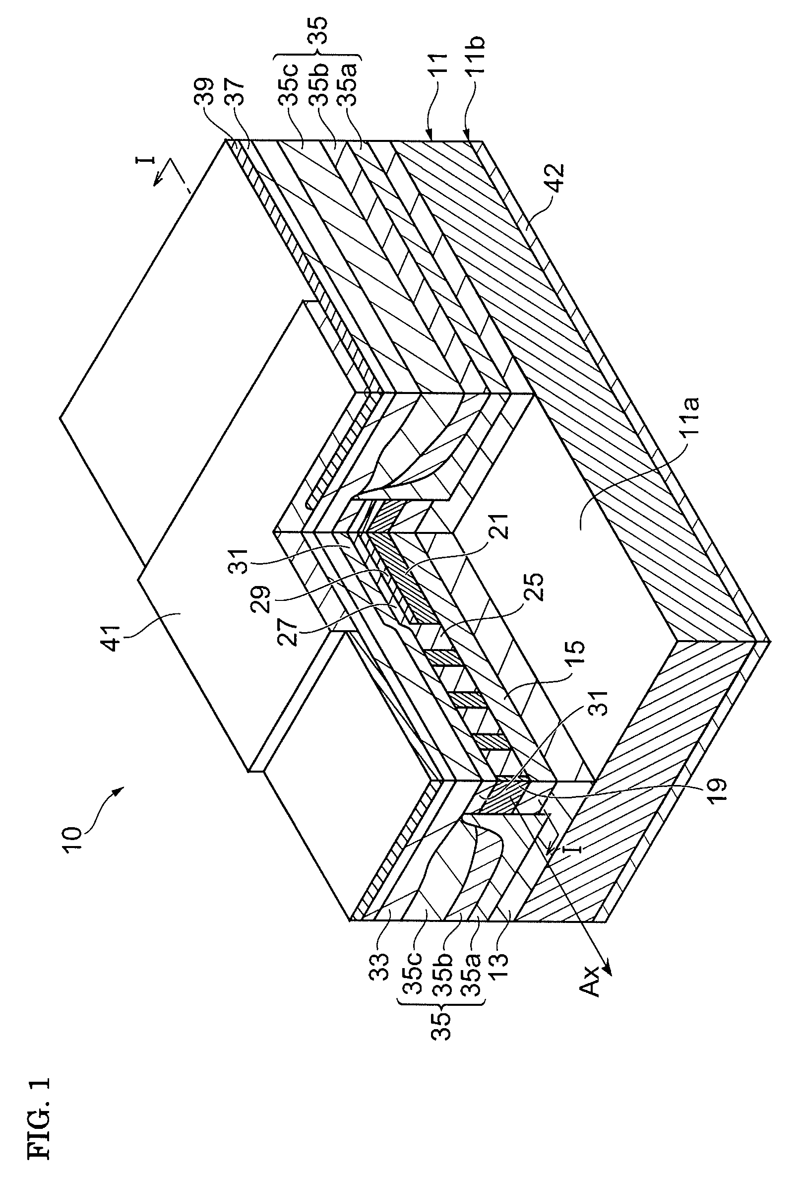
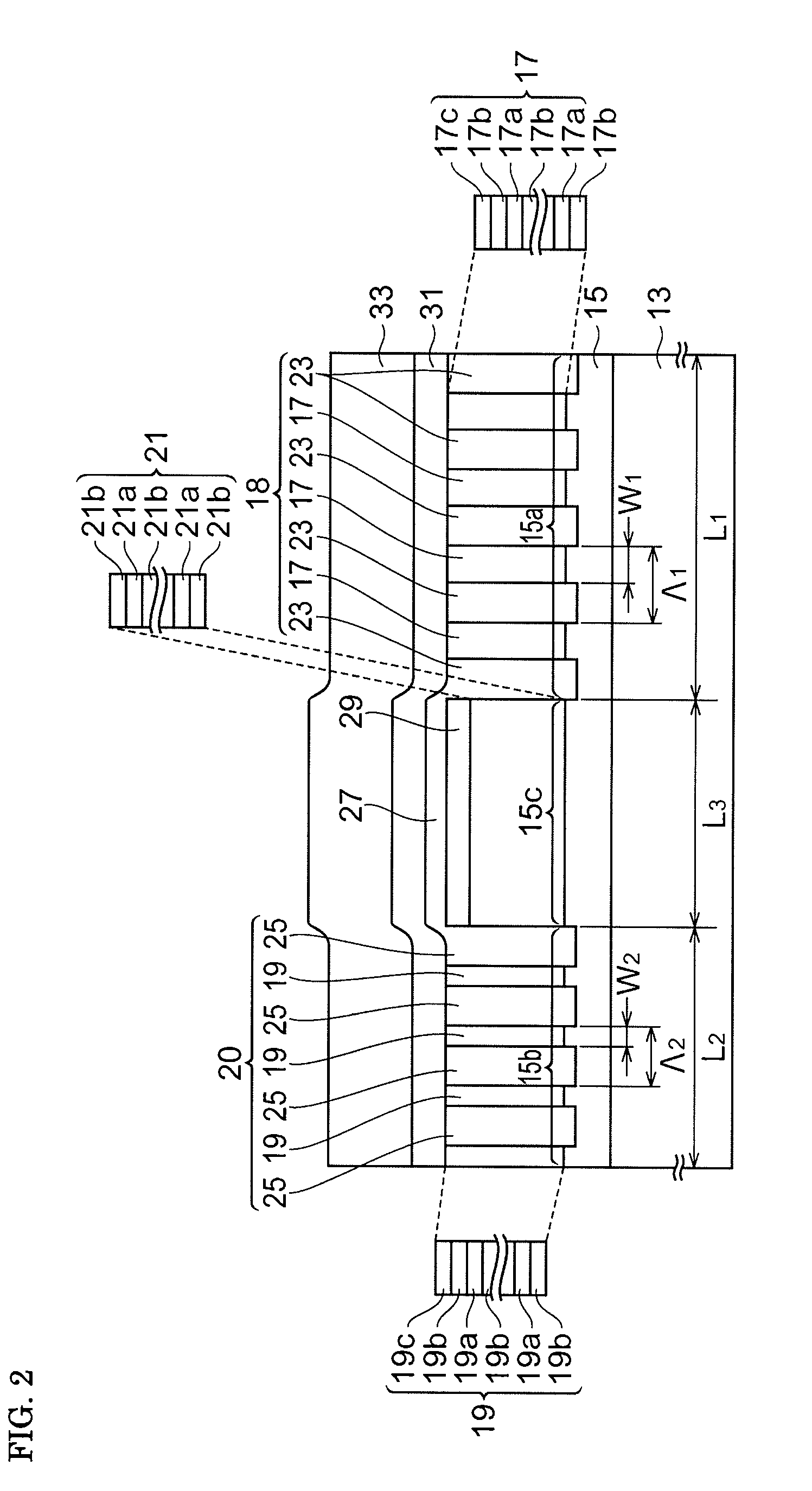
[0009]In this semiconductor laser, the first quantum wires and the buried semiconductor regions having a refractive index different from the refractive index of the first quantum wires are alternately arranged on the first area to constitute the first distributed Bragg reflector. Furthermore, the second quantum wires and the buried semiconductor regions having a refractive index different from the refractive index of the second quantum wires are alternately arranged on the second area to constitute the second distributed Bragg reflector. These distributed Bragg reflectors and the active layer constitute a laser cavity. Accordingly, the semiconductor laser of the present invention can realize a laser cavity without having a
butt joint structure. Since the laser cavity does not include the
butt joint structure,
optical coupling loss due to the butt joint structure can be decreased.
[0013]In this semiconductor laser, since the width of each of the first quantum wires in the direction of the predetermined axis is larger than the width of each of the second quantum wires in the direction of the predetermined axis, the
coupling coefficient of the first quantum wires is larger than the
coupling coefficient of the second quantum wires. In addition, since the product of the length of a distributed Bragg reflector and the
coupling coefficient contributes to the
reflectivity and the bandwidth of the stop-band, the
reflectivity of the first distributed Bragg reflector is higher than the
reflectivity of the second distributed Bragg reflector. Accordingly, the first distributed Bragg reflector functions as a reflector having a
high reflectivity, and a higher optical output can be obtained from a front
facet of the second distributed Bragg reflector. Furthermore, the bandwidth of the stop-band (reflection bandwidth) of the first distributed Bragg reflector is larger than the bandwidth of the stop-band (reflection bandwidth) of the second distributed Bragg reflector. Accordingly, in this semiconductor laser, the second distributed Bragg reflector functions as a
wavelength selective filter, and thus light emitted in a single
longitudinal mode can be easily obtained.
[0017]According to this semiconductor laser, the first quantum wires, the second quantum wires, and the active layer include well
layers composed of the same material and barrier
layers composed of the same material. Therefore, the first quantum wires, the second quantum wires, and the active layer include the same
semiconductor structure. The
absorption edge wavelength of the first and second first quantum wires is shorter than the
absorption edge wavelength of the active layer because the
absorption edge wavelength of the
quantum wire is shortened by the quantum effect. Thus, the first and second distributed Bragg reflectors function as optical waveguides with a low loss.
[0021]According to this semiconductor laser, a
valence band offset between the overflow prevention layer and the second optical confinement layer can be small, and thus the overflow prevention layer does not function as a substantial barrier for holes moving toward the active layer. Therefore, a semiconductor laser having satisfactory characteristics can be obtained. On the other hand, at the
conduction band side, the overflow prevention layer functions as a potential barrier for electrons moving from the active layer because of a difference in the magnitude of the band-gap energy. Accordingly, overflow of electrons from the active layer can be suppressed, and thus a semiconductor laser having satisfactory temperature characteristics can be obtained.
[0027]In the method of the present invention, an arrangement of the plurality of first quantum wires and an arrangement of the plurality of second quantum wires are formed at both sides of the active layer along a predetermined axis. Each of the arrangements of the quantum wires functions as a distributed Bragg reflector. The length of the arrangement of the quantum wires in the direction of the predetermined axis corresponds to the length of the distributed Bragg reflector. The width of each of the first quantum wires is different from the width of each of the second quantum wires, and thus the coupling coefficient of the first quantum wires is larger than the coupling coefficient of the second quantum wires. In addition, the product of the length of a distributed Bragg reflector and the coupling coefficient contributes to the reflectivity and the bandwidth of the stop-band. Therefore, the distributed Bragg reflector formed by the first quantum wires can have a reflectivity higher than the reflectivity of the distributed Bragg reflector formed by the second quantum wires. Accordingly, the distributed Bragg reflector formed by the first quantum wires functions as a reflector having a
high reflectivity. On the other hand, the bandwidth of the stop-band of the distributed Bragg reflector formed by the second quantum wires is smaller than the bandwidth of the stop-band of the distributed Bragg reflector formed by the first quantum wires. A plurality of longitudinal
modes are included in the stop-band of the distributed Bragg reflector formed by the first quantum wires, and threshold gains of these longitudinal
modes are decreased. Among these longitudinal
modes, only the threshold
gain of a
longitudinal mode included also in the stop-band of the distributed Bragg reflector formed by the second quantum wires is further decreased. Only this
longitudinal mode is selected and emitted as a single oscillation mode. Accordingly, the distributed Bragg reflector formed by the second quantum wires functions as a
wavelength filter, and thus this semiconductor laser operates in a single longitudinal mode. The width of the quantum wires can be controlled by changing the pattern shape of the
mask. Furthermore, the length of a distributed Bragg reflector constituted by a plurality of quantum wires in the direction of the predetermined axis can also be controlled by changing the pattern shape. Thus, the reflectivity and the bandwidth of the stop-band of the distributed Bragg reflector can be easily controlled.
[0029]In the method of the present invention, the overflow prevention layer is grown on the active layer, and the second optical confinement layer is then grown thereon. The
valence band offset between the overflow prevention layer and the second optical confinement layer can be small, and thus the overflow prevention layer does not function as a substantial barrier for holes moving toward the active layer. Therefore, a semiconductor laser having satisfactory characteristics can be obtained. On the other hand, at the
conduction band side, the overflow prevention layer functions as a potential barrier for electrons moving from the active layer because of a difference in the magnitude of the band-gap energy. Accordingly, overflow of carriers (electrons) from the active layer can be suppressed, and thus a semiconductor laser having satisfactory temperature characteristics can be obtained. Furthermore, the buried semiconductor regions and the overflow prevention layer are formed at the same time by a common semiconductor growth process. Therefore, the preparation process can be simplified.


