Semiconductor thin film forming system

Inactive Publication Date: 2010-01-14
NEC CORP +1
View PDF3 Cites 17 Cited by
  • Summary
  • Abstract
  • Description
  • Claims
  • Application Information

AI Technical Summary

Benefits of technology

[0038]It is desired to enlarge the area to be processed while the irradiation intensity supplied per area is maintained not being increased. The effective way for achieving this purpose is to increase the optical energy supplied per a pulse. The pulse width of the optical source of the gas laser such as an eximer laser may be increased by enlarging the optical space. The cooling rate can be controlled by carrying out the irradiation by at least one pulse (the second pulse) which starts with a delay to the first pulse. The intensity of the second pulse used herein is relatively smaller than the intensity required for the melting and recrystallization (first pulse intensity) so that the output of the optical source used by the second pulse is smaller than that of the optical source of the first pulse. In other words, the optical source with a large output is used as the first pulse optical source to process the large area and the second and the subsequent pulses uses the optical source with smaller output (smaller irradiation intensity), which means the laser with the smaller pulse width, such that the cooling rate is effectively controlled. It is thus possible to provide an apparatus which achieves efficient price performance.
[0041]Next, the case where a delayed second laser light is irradiated with a delay relative to a first laser light. As is described above, a laser light at a late light emission stage suppresses the increase of the cooling rate, and the cooling rate after the completion of light emission controls the crystallization. The last supplied energy is supposed to initialize precedent cooling processes. Specifically, by supplying an additional energy, a precedent cooling process is once initialized and a solidification process is repeated again, even if the crystal becomes amorphous or microcrystalline in the precedent cooling process. This is provably because the interval of light irradiation is very short of the order of nanoseconds, and loss of the energy by thermal conduction to the substrate and radiation to the atmosphere is small. The energy previously supplied therefore remains nearly as intact. In this assumption, a long time interval sufficient to dissipate heat is not considered. Accordingly, by controlling the cooling rate after the completion of a second heating by the additionally supplied energy, the crystal is expected to grow satisfactorily. As shown in FIG. 14, the cooling rate is controlled to a desired level by controlling the delay time of the second laser irradiation.

Problems solved by technology

A conventional tab connection method or wire bonding method cannot significantly provide such a decreased connection pitch.
However, if a process at high temperatures as in the above case is employed in the polycrystalline silicon TFT process, low softening point glasses cannot be employed.
The resulting polycrystalline silicon thin film and polycrystalline silicon thin film transistor cannot therefore have satisfactorily uniform characteristics.
However, according to this process, a weak light is rather oscillated even though the formation of spiking is inhibited.
The resulting transistor element and thin film integrated circuit cannot have a significant uniformity in the substrate plane.
However, although this process can stably irradiate the substrate with a laser beam, the process also yields increased excess lasing that does not serve to the formation of a polycrystalline silicon thin film.
The productivity is decreased from the viewpoint of the life of an expensive laser source and an excited gas, and the production efficiency of the polycrystalline silicon thin film is deteriorated with respect to power required for lasing.
The production costs are therefore increased.
When a substrate to be exposed to laser is irradiated with an excessively strong light as compared with a target intensity, the substrate will be damaged.
Such an excessively strong light is induced by an irregular irradiation intensity.
In LCDs and other imaging devices, a light passing through the substrate scatters in an area where the substrate is damaged, and the quality of image is deteriorated.
However, as pointed out in the above reference, such an increased irradiation energy invites the resulting film to become amorphous or microcrystalline.
Particularly, when the cooling rate in cooling procedure is extremely large and the material undergoes an excessive supercooling, the material is not crystallized at around its solidification point, and becomes an amorphous solid due to quenching and rapid solidification.

Method used


Image

  • Semiconductor thin film forming system
  • Semiconductor thin film forming system
  • Semiconductor thin film forming system

Examples


Embodiment Construction

[0061]The embodiments of the invention will now be illustrated in detail with reference to the drawings.

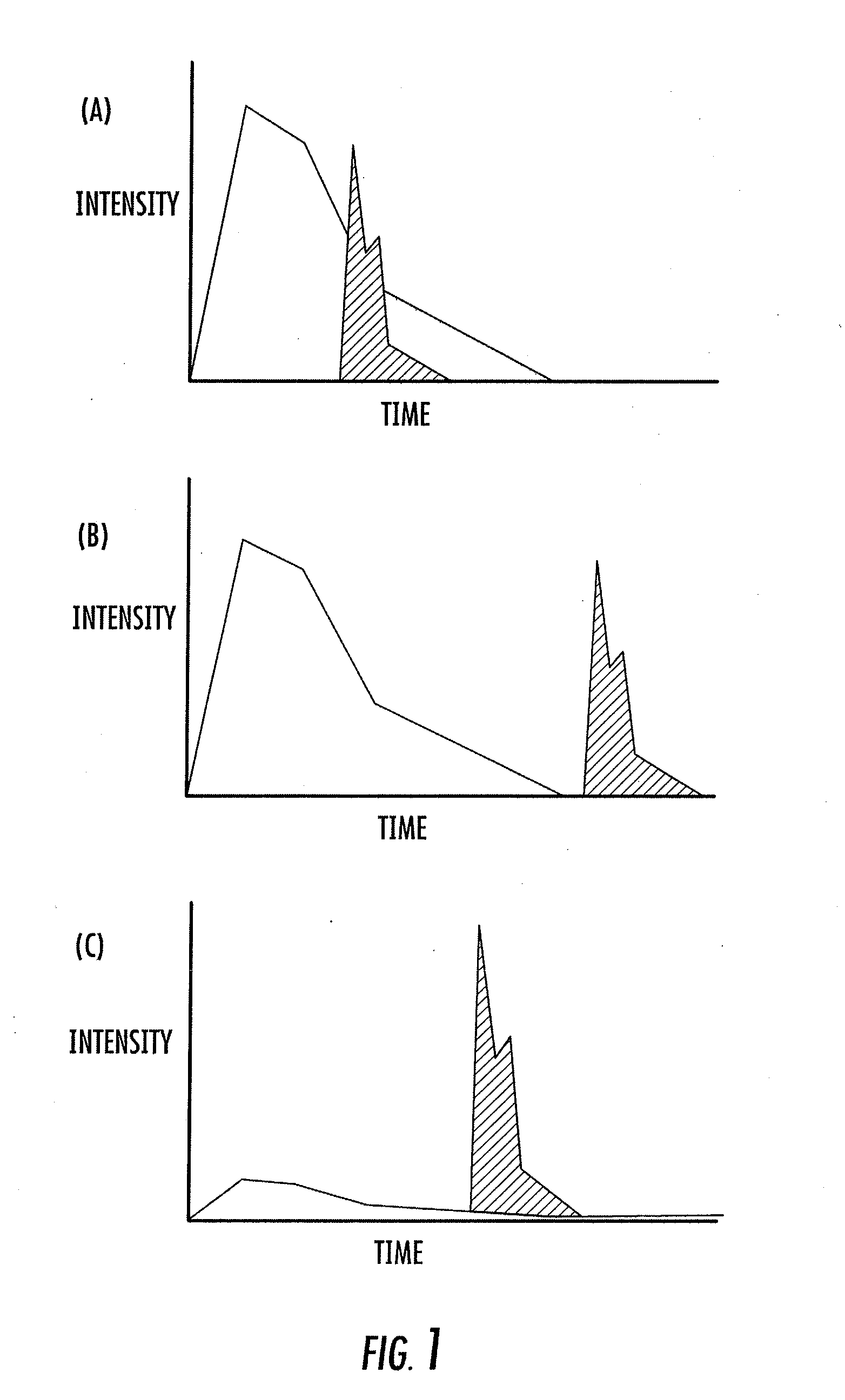
[0062]FIG. 1 illustrates an example of the embodiment of the present invention. Each of the oscillation start timings is depicted as the abscissa axis while the irradiation energy (i.e., the intensity of pulse irradiation) is depicted as the region bound by the pulse line. FIG. 1(a) shows an example where a second pulse is irradiated with a delay to a first pulse laser. FIG. 1(b) shows an example where a second pulse is irradiated after the completion of the first pulse irradiation. Depending on the constitution of the laser apparatus, the time interval required between the supply of the trigger signal for controlling the oscillation and the actual start of the oscillation. Therefore, it is preferred to calculate and predetermine the “trigger oscillation” time in advance so as to control the irradiation to be started at the simultaneous timing. As compared with the second pulse, t...


PUM

PropertyMeasurementUnit
Densityaaaaaaaaaa
Widthaaaaaaaaaa
Irradiation doseaaaaaaaaaa

Abstract

A thin film processing method for processing the thin film by irradiating the optical beam to the thin film, wherein one set of irradiation includes the first optical pulse irradiation to the thin film and the second optical pulse irradiation to the thin film which substantially starts with a delay to the first optical pulse irradiation, the one set of irradiation being repetitively carried out for processing the thin film, and the relationship between the first and the second pulse satisfies (the pulse width of the first optical pulse)>(the pulse width of the second optical pulse). Preferably, the relationship between the first and the second pulse satisfies (the irradiation intensity of the first optical pulse)≧(the irradiation intensity of the second optical pulse). A silicon thin film with a small trap state density is thus manufactured by the optical irradiation.

Description

CROSS REFERENCE TO RELATED APPLICATIONS[0001]This application is a divisional of U.S. application Ser. No. 10 / 276,553 filed Jul. 3, 2003, which is a §371 of PCT / JP2001 / 04112, filed May 17, 2001, which claims priority from Japanese Application No. 2000-144363, filed May 17, 2000, the entire contents of each of these applications being incorporated herein by reference in their entirety.BACKGROUND OF THE INVENTION[0002]1. Field of the Invention[0003]This invention relates to a system for the formation of a silicon thin film and a good-quality semiconductor-insulating film interface. Such silicon thin films are used for crystalline silicon thin film transistors, and such semiconductor-insulating film interfaces are employed for field effect transistors. The invention also relates to a semiconductor thin film forming system by the pulsed laser exposure method. In addition, the invention relates to a system for the manufacture of driving elements or driving circuits composed of the semico...

Claims


Application Information

Patent Timeline
IPC IPC(8): G21G5/00H01L21/20H01L21/208H01L21/268H01L21/336H01L29/786
CPCB23K26/0604H01L21/2026B23K26/0656B23K26/0613B23K26/066H01L21/0262H01L21/02592H01L21/02683H01L21/02686H01L21/02422H01L21/02488H01L21/02678H01L21/02532H01L21/02598H01L21/02691H01L21/26
Inventor TANABE, HIROSHITANEDA, AKIHIKO
Owner NEC CORP
Why Eureka
Try Eureka