
NANO complex oxide doped dielectric ceramic material, preparation method thereof and multilayer ceramic capacitors made from the same

Inactive Publication Date: 2009-05-28
TSINGHUA UNIV
View PDF22 Cites 30 Cited by
  • Summary
  • Abstract
  • Description
  • Claims
  • Application Information

AI Technical Summary

Benefits of technology

[0031]The nano complex oxide doped dielectric ceramic material is mixed with suitable organic solvent, binder, dispersant and plasticizer to provide a ceramic slurry; a dielectric layer is formed by a tape-casting method using the slurry with the thickness of the dielectric layer of below 10 μm; multiple of the dielectric layers and base-metal internal electrode layers are alternately stacked to prepare a stack body; the binder is removed after the stacked body is formed; the binder-removed stack body is then sintered under a reducing atmosphere at a temperature of from 950° C. to 1250° C.; the stack body is then reoxidized in a weak oxidation atmosphere at 800° C.˜1100° C. to enhance insulation resistance of the dielectric; and then the stack body is cooled down to room temperature and Cu or Ag terminal electrode is mounted to obtain an ultrafine-grained and temperature-stable multilayer ceramic capacitor having base-metal internal electrodes.

Problems solved by technology

However, use of such noble metals becomes a barrier to cut down the production cost of multilayer ceramic capacitors.
However, if such base metals are used as a material for internal electrodes and fired in the conventional firing conditions of the dielectric ceramic materials, they would be oxidized easily and lose functions as the internal electrodes.
However, this dielectric ceramic composition is of no practical use since its insulation resistance and temperature coefficient of capacitor are affected by the grain size of the main component BaTiO3, thus making it difficult to control the composition to obtain stable dielectric properties.
However, the sintering temperature for this system is too high, over 1300° C. and the TCC at −55° C. or 125° C. is near −15%.
Thus, the composition is not suitable for industrial production.
However, the reducing of the grain size generally induces the decreasing of the dielectric constant.

Method used


Image

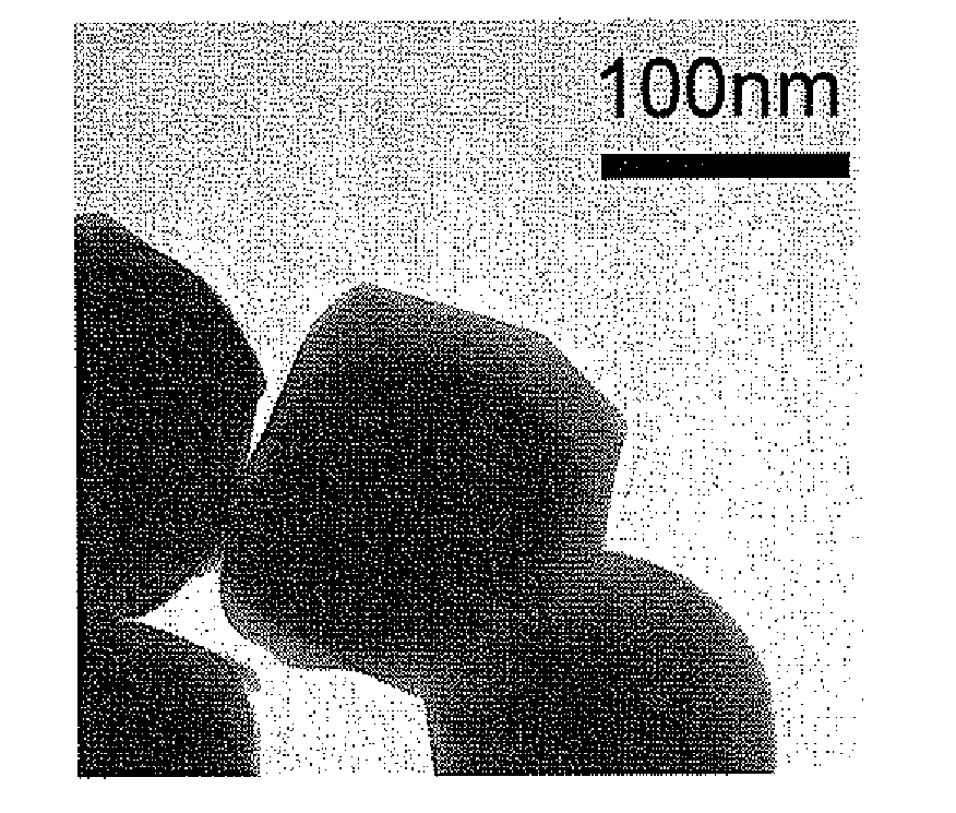
  • NANO complex oxide doped dielectric ceramic material, preparation method thereof and multilayer ceramic capacitors made from the same
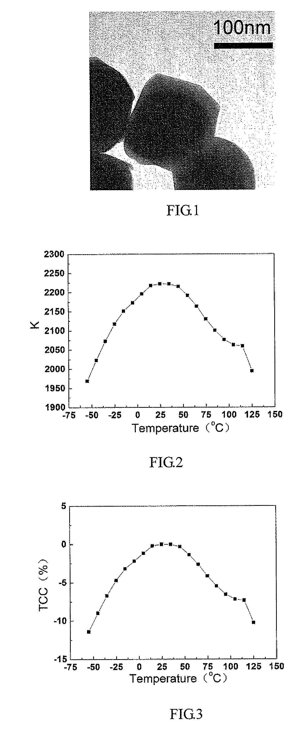
  • NANO complex oxide doped dielectric ceramic material, preparation method thereof and multilayer ceramic capacitors made from the same
  • NANO complex oxide doped dielectric ceramic material, preparation method thereof and multilayer ceramic capacitors made from the same

Examples


example 1

Preparation of a Nano Complex Oxide Doped Dielectric Ceramic Material through a Chemical Coating Process

[0056]BaTiO3 powders (with an average particle size of 120 nm) were ball-milled in ethanol for 12 hours to get a BaTiO3 slurry A; Nitrates corresponding to the oxides in the nano complex oxide were weighed according to molar ratios of Y:Ce:Mn:Mg:Si:Ca=4:1:3:12:5:3 and dissolved in deionized water to obtain a clear solution B; Si(OEt)4, ethanol, acetic acid and deionized water were mixed by volume ratios of Si(OEt)4:ethanol:acetic acid:deionized water=1:10:6:20 to obtain a clear and stable solution C; solution B and solution C were dropwise added to the BaTiO3 slurry A by volume ratios of A:B:C=5:2:1; Ammonia water was added to make the pH to 8 so that the doping elements were coated on to the surface of the BaTiO3 particles through a co-precipitation process; the obtained slurry was dried and then was sintered at 500° C. for 2 hours, followed by sieving to obtain a nano complex ox...

example 2

[0057]Nano complex oxide doped dielectric ceramic materials were prepared by the same way as described in example 1 except that the average particle sizes of the BaTiO3 powders were 120 nm, 135 nm and 150 nm, respectively, the composition of the nano complex oxide dopant in the coating layer (CL) was Y:Ce:Mn:Mg:Si:Ca=3:2:3:12:4:2 (molar ratio), and the molar ratio of the BaTiO3 to the nano complex oxide was 95:5. Thus samples 1˜3 of the nano complex oxide doped dielectric ceramic materials were obtained, as shown in Table 1.

[0058]Tests of the dielectric properties of samples 1˜3.

[0059]Each of samples 1˜3 was pressed into a pellet with a diameter of 10 mm and sintered in a reducing atmosphere at 1200° C. for 2 h (N2:H2=30:1), followed by reoxidizing in a weak oxidation atmosphere at 1050° C. for 2 h. Silver electrodes were deposited onto both the main sides of the pellet to conduct dielectric measurement. The dielectric properties and grain size of these samples are listed in Table 1...

example 3

[0060]Nano complex oxide doped dielectric ceramic materials were prepared by the same way as described in example 1 except that the average particle sizes of the barium titanate, the mole ratios of barium titanante to the nano complex oxide and the compositions of the nano complex oxides in the coating layer (CL) were different, as listed in Table 2 and Table 3 Thus samples 4˜9 of nano complex oxide doped dielectric ceramic materials were obtained.

[0061]Tests of the dielectric properties of samples 4˜9.

[0062]Each of samples 4˜9 was pressed into a pellet with a diameter of 10 mm and sintered in a reducing atmosphere at 1150° C.˜1250° C. for 2 h (N2:H2=35:1), followed by reoxidizing in a weak oxidation atmosphere at 1050° C. for 3 h. Silver electrodes were deposited onto both the main sides of the pellet to conduct dielectric measurement. The dielectric properties and the average grain sizes of these samples are listed in Table 3.

TABLE 2Nano complex oxidein the coating layerCompositio...


PUM

PropertyMeasurementUnit
Grain sizeaaaaaaaaaa
Temperatureaaaaaaaaaa

Abstract

The present invention provides a nano complex oxide doped dielectric ceramic material used for a multilayer ceramic capacitor using a base metal as a material of internal electrodes. The doped dielectric ceramic material comprises barium titanate and a nano complex oxide dopant, wherein the molar ratio of the barium titanate to the nano complex oxide dopant is in the range of (90˜98):(2˜10), the average particle size of the barium titanate is 50˜300 nm and the nano complex oxide dopant has the following formula (1): w A+x B+y C+z D. The present invention also provides processes for preparing the nano complex oxide doped dielectric ceramic material and ultrafine-grained and temperature-stable multilayer ceramic capacitors using the nano complex oxide doped dielectric ceramic material as the material of dielectric layers.

Description

TECHNICAL FIELD OF THE INVENTION[0001]The present invention relates to a dielectric ceramic material. Particularly, the present invention relates to a nano complex oxide doped dielectric ceramic material used for an ultrafine grained and temperature-stable multilayer ceramic capacitors employing a base metal such as nickel as the material of internal electrodes.TECHNICAL BACKGROUND[0002]With rapid development of various types of electronic devices, there is a tendency that these devices and products are smaller in size and larger in capacitance. The component parts for these devices are also increasingly produced in compact and lightweight design. The means for mounting the electronic components are also changing to surface mounting technology (SMT). Small components such as capacitor and resistor are called “chip components”.[0003]Multilayer Ceramic Capacitor (MLCC) is a widely used typical chip component. It is generally fabricated by forming alternating layers of an internal elec...

Claims


Application Information

Patent Timeline
IPC IPC(8): H01G4/12C04B35/468B29C71/02B05D5/12
CPCC04B2235/3229C04B35/462C04B2235/3262C04B2235/3418C04B2235/441C04B2235/443C04B2235/449C04B2235/5445C04B2235/5454C04B2235/6025C04B2235/656C04B2235/6567C04B2235/6582C04B2235/6584C04B2235/663C04B2235/785H01G4/1227H01G4/30B82Y30/00C01G23/006C01P2002/52C01P2004/04C01P2004/62C01P2004/64C01P2006/32C01P2006/40C04B35/4682C04B35/624C04B35/62805C04B35/62807C04B35/6281C04B35/62815C04B35/62886C04B35/62897C04B35/632C04B35/638C04B2235/3206C04B2235/3208C04B2235/3225C04B35/46C04B2235/3236C04B37/001C04B37/006B32B18/00H01G4/33H01G4/1218C04B2237/346C04B35/468C04B35/6261C04B35/62625C04B35/62635C04B35/628
Inventor WANG, XIAOHUITIAN, ZHIBINWANG, TIANLI, LONGTU
Owner TSINGHUA UNIV
Learn More