
Film growth system and method

a film growth and film technology, applied in the direction of liquid/solution decomposition chemical coating, transportation and packaging, coatings, etc., can solve the problems of limiting electrical performance characteristics, non-stoichiometric proportions, and deposited films often include relatively high defect densities, so as to improve physical, chemical, optical, and easy control

Inactive Publication Date: 2008-12-04
QUANTUMSCAPE CORP
View PDF6 Cites 26 Cited by
  • Summary
  • Abstract
  • Description
  • Claims
  • Application Information

AI Technical Summary

Benefits of technology

[0012]Objects of the invention include the following: providing a bath deposition apparatus capable of depositing a selected phase on a substrate while minimizing homogeneous nucleation of the same or similar phase within the bulk of the fluid bath; providing a bath deposition apparatus capable of depositing films having improved physical, chemical, optical, or electrical properties; providing a bath deposition apparatus that is more easily controlled; providing a bath deposition apparatus that uses reagents more efficiently; providing a bath deposition apparatus that allows localized heating of a relatively small volume of the bath while maintaining the remainder of the bath at a relatively lower temperature; providing a method for bath deposition that is more easily controlled; providing a method for bath deposition that minimizes homogeneous nucleation within the bath; providing a method for bath deposition capable of depositing films of selected II-VI compounds, other compounds, or metals having improved properties. These and other objects will become apparent on reading the specificati

Problems solved by technology

), are non-equilibrium, often resulting in non-stoichiometric proportions.
Also, due to the nature of the deposition processes, the deposited films often include relatively high defect densities.
In the case of semiconducting devices, such high defect levels can limit electrical performance characteristics.
In semiconductor device fabrication wherein p-n junctions are formed in a partial vaccuum by depositing one film over a second film or a substrate of different conductivity type, the conventional evaporative and sputtering techniques may provide unsatisfactory film qualities.
As an alternative, relatively more expensive techniques such as Chemical Vapor Deposition (CVD), Molecular Beam Epitaxy (MBE), pulsed laser deposition, and atomic layer epitaxy, are useful, especially with formation of III-V compound semiconductor materials, but satisfactory deposition processes have not been available for fabrication of thin film II-VI compound semiconductor materials.
However, the technique has provided low growth rates, e.g., 20 to 30 Å / minute, and the grown film thickness per bath cycle is limited to around 1000 Å rendering it non-suitable for volume manufacture.
With traditional chemical bath deposition techniques, efforts to increase film growth rates typically result in degradation of film quality.
This, of course, is time consuming and generally can be an expensive endeavor, wherein relatively expensive chemicals are wasted due to deposition of film materials on unwanted surfaces such as the equipment.
Particulates represent not only a waste of reagents but also a source of defects in the deposited film.
First, using a single complexing agent (generally taught to be NH4OH) prevents adequate process control: at a low concentration the solution is so unstable that unwanted homogeneous nucleation can occur, whereas at high concentration the activation energy required to form the film becomes so high that the claimed substrate temperature may not be able to overcome it to cause a film growth.
Second, the thickness of film that can be grown in a single step is very small, so to grow a film of 0.1 μm or greater, multiple cycles are needed and this will tend to introduce greater concentrations of defects.
This will also make the process cumbersome and less manufacturing friendly.
The use of NH2CONH2 as a single ligand will result in excessive homogenous reaction, and ZnO film growth takes place mostly by particulate adsorption.
ZnO so formed is less transparent and of little or no practical use.
Furthermore, the side of the substrate next to the incoming solution gets the full dose of the solution, hence high growth rate, whereas the side of the substrate at solution exit receives the least dose, hence low growth rate.
As a result, the film non-uniformity will increase with increasing substrate size.
Since all the flowing solution sees the heat provided by the substrate, film growth will take place on the substrate plus any part of the system on contact with the hot growth solution, leading to material waste.
If the particulate generation happens in the enclosed chamber, these could be trapped and get adsorbed unto the substrate, leading to poor quality film.
This arrangement forces the hot growth solution to be in contact with the substrate and substantial part of the chamber system, and results in wasteful film growth on unwanted areas.
The latter will also increase the cost of keeping the chamber clean to prevent particle build up.
Subjecting a relatively large volume of growth solution in chamber at high pressure and temperature will not only encourage the desired heterogeneous reaction responsible for film growth but also substantially increase the unwanted homogenous reaction; the latter will lead to fast depletion and waste of material, and this will in turn increase the production cost.
However, for semiconductor film deposition needed for solar cells and other optoelectronics applications where the required film thickness is more than 1000 Å, the high temperature bulk deposition step time will be longer and the instantaneous heating and cooling will not help.
One would therefore expect the growth rate on the substrate as well as other parts of the chamber system in contact with the hot solution to be about same; the consequence of this is substantial material waste.
This will make the chamber cleanliness even a much bigger challenge.
The operating cost and waste management in using this system for semiconductor film manufacturing will be prohibitive.
It should also be noted that this approach is only applicable to rigid substrates; flexible substrates cannot be used.

Method used


Image

  • Film growth system and method
  • Film growth system and method
  • Film growth system and method

Examples


Embodiment Construction

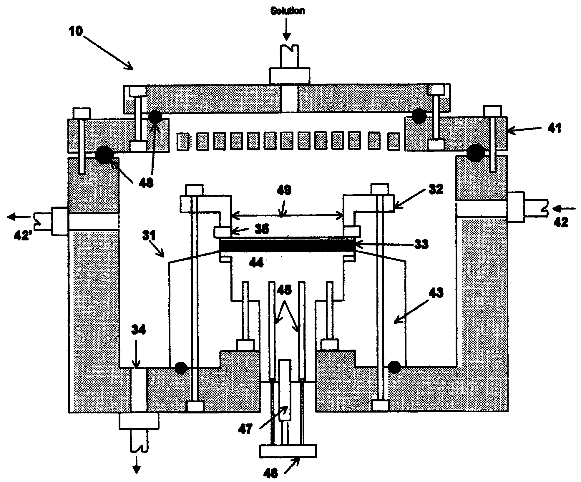
[0034]There has been a need for a chemical system that can create high quality films, e.g., semiconductor films, at high formation rates, while providing a relatively uniform film thickness across the entire substrate surface over which the film is formed. In accordance with several embodiments of the invention, such a high quality semiconductor film is formed by a replacement reaction wherein the system provides a continuous or replenishable supply of chemical processing solution. In several examples, the solution reacts about the surface of a heated substrate. The substrate temperature may be controlled to exhibit a substantially uniform temperature across the surface. That is, temperature differentials along the surface over which the film is formed are limited in order to effect a substantially constant reaction rate along the surface, thereby assuring a relatively uniform film growth rate. Further, the pH and composition of the solution may be continuously monitored and maintai...


PUM

PropertyMeasurementUnit
Temperatureaaaaaaaaaa
Lengthaaaaaaaaaa
Lengthaaaaaaaaaa

Abstract

An apparatus for depositing a solid film onto a substrate from a reagent solution includes a reservoir of reagent solution maintained at a sufficiently low temperature to inhibit homogeneous reactions within the reagent solution. The reagent solution contains multiple ligands to further control temperature stability and shelf life. The chilled solution is dispensed through a showerhead onto a substrate. The substrate is positioned in a holder that has a raised structure peripheral to the substrate to retain or impound a controlled volume (or depth) of reagent solution over the exposed surface of the substrate. The reagent solution is periodically or continuously replenished from the showerhead so that only the part of the solution directly adjacent to the substrate is heated. A heater is disposed beneath the substrate and maintains the substrate at an elevated temperature at which the deposition of a desired solid phase from the reagent solution may be initiated. The showerhead may also dispense excess chilled reagent solution to cool various components within the apparatus and minimize nucleation of solids in areas other than on the substrate. The apparatus and its associated method of use are particularly suited to forming films of II-VI semiconductors.

Description

CROSS REFERENCE TO RELATED APPLICATION[0001]This application claims the benefit of Provisional Application Ser. No. 60 / 940,797 filed by the present inventor on May 30, 2007, the entire disclosure of which is incorporated herein by reference.BACKGROUND OF THE INVENTION[0002]1. Field of the Invention[0003]The invention pertains to a system and method for chemically coating a variety of surfaces with semiconductor materials, metals, or insulators for various applications including electronics.[0004]2. Description of Related Art[0005]Numerous coating processes are commonly employed in industrial applications, including electroless chemical, chemical vapor and physical vapor depositions. Physical vapor deposition is commonly used in semiconductor manufacturing applications, often employing expensive vacuum techniques in order to sustain a relatively high film growth rate. Many such processes, while performed at high temperatures (e.g., greater than 300° C.), are non-equilibrium, often re...

Claims


Application Information

Patent Timeline
IPC IPC(8): H01L21/208B05C5/00
CPCC23C18/06Y10T428/12528C23C18/1241C23C18/1275C23C18/1279C23C18/1283H01L21/02554H01L21/02565H01L21/02573H01L21/02628H01L21/67207H01L21/6838H01L21/68785H01L29/22C23C18/1216
Inventor OLADEJI, ISAIAH O.
Owner QUANTUMSCAPE CORP
Learn More