
Growth/fabrication of organic-inorganic quasi phase-matching structures for frequency conversion devices

a quasi-phase-matching structure and frequency conversion technology, applied in the direction of crystal growth process, semiconductor laser, instruments, etc., can solve the problems of difficult, costly and time-consuming process for fabricating such op templates, and achieve the effects of wide range of transparency, high nonlinear susceptibility, and cost-effective process

Active Publication Date: 2020-02-04
THE UNITED STATES OF AMERICA AS REPRESETNED BY THE SEC OF THE AIR FORCE
View PDF4 Cites 0 Cited by
  • Summary
  • Abstract
  • Description
  • Claims
  • Application Information

AI Technical Summary

Benefits of technology

The present invention combines the advantages of inorganic semiconductor materials and organic crystalline materials, which have high nonlinear susceptibilities and a broad range of transparency. The use of homo- or heteroepitaxially grown semiconductor layers deposited on a half-patterned crystalline inorganic template in combination with an organic crystal material filling the inorganic matrix using various growth techniques eliminates the need for orientation-patterned templates, making the fabrication process easier and more cost-effective. Additionally, it also eliminates the need for thick epitaxial growth on orientation-patterned templates, which often requires many efforts to establish the optimal growth conditions for a new material. The invention simplifies the entire process and reduces the likelihood of parasitic nucleation, resulting in high-quality structure for various applications.

Problems solved by technology

The fabrication of such OP templates is a difficult, costly and time-consuming process.

Method used


Image

  • Growth/fabrication of organic-inorganic quasi phase-matching structures for frequency conversion devices
  • Growth/fabrication of organic-inorganic quasi phase-matching structures for frequency conversion devices
  • Growth/fabrication of organic-inorganic quasi phase-matching structures for frequency conversion devices

Examples


second embodiment

[0093]With regard to the invention, inorganic, semi-organic and organic electret nonlinear materials—crystalline, polycrystalline, and amorphous (e.g. glasses and polymers)—have some indisputable advantages in comparison to their inorganic counterparts. Such advantages include their higher (some times more than one order of magnitude higher) nonlinear susceptibility and ultrafast response that allows the achievement of much larger nonlinear optical (NLO) efficiency. In addition, they can be grown from solutions, melts and vapors at relatively low temperatures—usually less than 300° C., even <100° C., using a number of different relatively simple and affordable techniques. However, the development of organic materials, which can be divided into two parts, i.e. organic crystals and organic polymers, also has its own issues briefly described below.

[0094]For high-speed second-order NLO applications, such as electro-optics (EO), second-harmonic generation (SHG), optical parametric oscill...

first embodiment

[0095]The preparation of inorganic semiconductor materials for nonlinear optical applications is expensive and complex, while organic materials are much cheaper and, due to their lower melting points, can be prepared or grown in less-energy consuming processes using simpler and relatively low-tech equipment. The growth techniques for most inorganic materials require the use of poisonous, flammable and corrosive gases such as arsine and phosphine. In contrast, neither the inorganic materials of the present invention, nor the processes of their fabrication contain or use dangerous chemicals. The preparation of orientation-patterned templates based on inorganic semiconductors itself is a complex, time-consuming process that often requires the use of expensive scientific equipment such as MBE (molecular beam epitaxy). In addition, the prior art template preparation process for OP templates of one material is not a universal process but rather a unique technique for each particular inorg...

third embodiment

[0130]Because of the miniature size of the structure, it is possible for the QPM matrix to be placed within a Second Harmonic Generation (SHG) device and even in an OPO (Optical Parametric Oscillator) optical set, according to the invention. Thus the whole polarization procedure may be directly performed in-situ, tuning the polarization by additional light “chargings” or / and partly electrical “dischargings” until achieving a maximal output.

[0131]The nonlinear susceptibility of many electrets is significantly higher than the traditional nonlinear susceptibility of the inorganic semiconductor materials such as GaP, GaAs, ZnSe, GaN, etc. The refractive index of the electrets is usually smaller. This means that one can expect self-focusing of the beams propagating throughout the structure (FIGS. 12A-12C). FIGS. 12A-12C illustrate structures having alternating layers of inorganic materials and organic / electret materials, as described above in the various embodiments. FIG. 12 A illustrate...


PUM

PropertyMeasurementUnit
thickaaaaaaaaaa
wavelengthsaaaaaaaaaa
temperaturesaaaaaaaaaa

Abstract

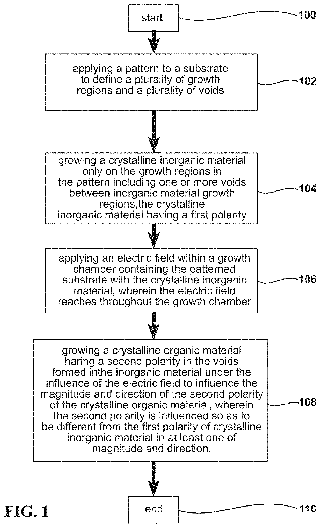
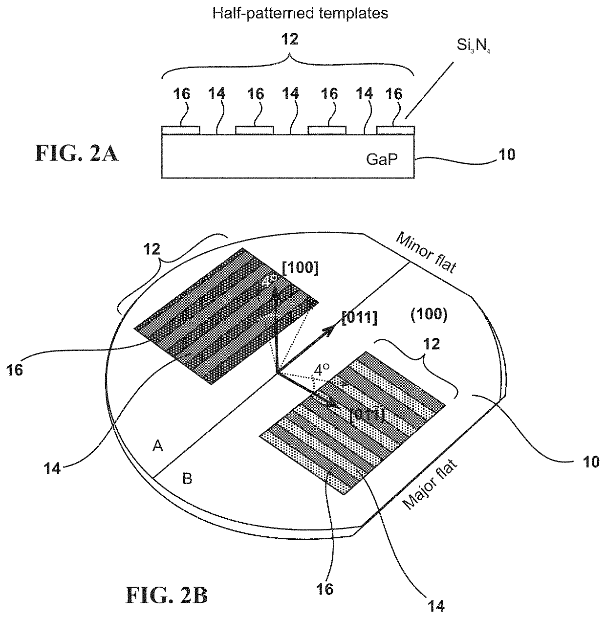
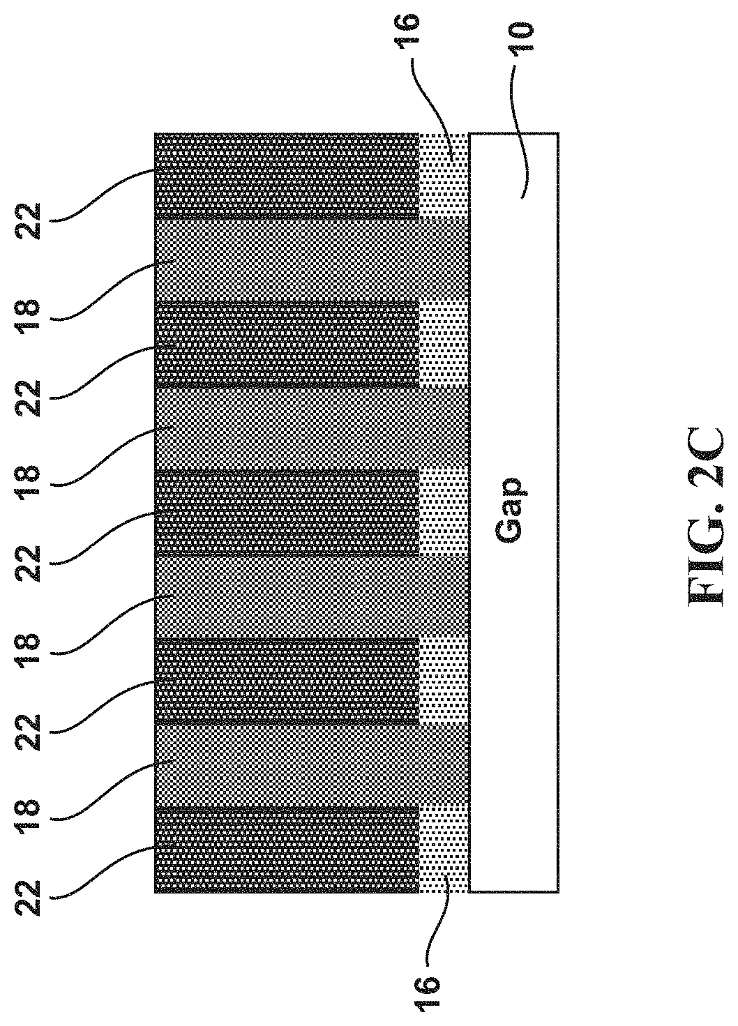
A method of making a quasi-phase-matching (QPM) structure comprising the steps of: applying a pattern to a substrate to define a plurality of growth regions and a plurality of voids; growing in a growth chamber a crystalline inorganic material on only the growth regions in the pattern, the crystalline inorganic material having a first polarity; applying an electric field within the growth chamber containing the patterned substrate with the crystalline inorganic material, wherein the electric field reaches throughout the growth chamber; and growing a crystalline organic material having a second polarity in the voids formed in the inorganic material under the influence of the electric field to influence the magnitude and the direction of the second polarity of the crystalline organic material, wherein the second polarity of the crystalline organic material is influenced to be different from the first polarity of the crystalline inorganic material in magnitude and / or direction.

Description

RIGHTS OF THE GOVERNMENT[0001]The invention described herein may be manufactured and used by or for the Government of the United States for all governmental purposes without the payment of any royalty.[0002]Pursuant to 37 C.F.R. § 1.78(a)(4), this application claims the benefit of and priority to prior filed Non-Provisional application Ser. No. 15 / 350,369, filed Nov. 14, 2016, which is expressly incorporated herein by reference.FIELD OF THE INVENTION[0003]The present invention relates generally to quasi-phase-matching structures and, more particularly, to the growth of organic-inorganic quasi-phase-matching structures which may be incorporated into frequency conversion devices.BACKGROUND OF THE INVENTION[0004]Coherent laser sources radiating in the mid- and longwave IR and THz wavelength ranges are in great demand due to their suitability for a wide variety of military and commercial applications, i.e., defense, security, science, industry, and medicine. However, such lasers are not...

Claims


Application Information

Patent Timeline
Patent Type & Authority Patents(United States)
IPC IPC(8): H01S5/06C30B30/02C30B25/04
CPCH01S5/0604C30B25/04C30B30/02H01S2304/00C30B29/54G02F1/3544G02F1/3548
Inventor TASSEV, VLADIMIR
Owner THE UNITED STATES OF AMERICA AS REPRESETNED BY THE SEC OF THE AIR FORCE
Learn More