
Process for forming low defect density heterojunctions

a technology of heterojunctions and semiconductors, applied in the direction of semiconductor devices, electrical equipment, basic electric elements, etc., can solve the problems of excess leakage from the gate to the channel of the transistor, defects at certain heterojunctions, etc., to minimize the nucleation of morphological defects and low defect density

Inactive Publication Date: 2010-10-26
TELEDYNE SCI & IMAGING
View PDF9 Cites 0 Cited by
  • Summary
  • Abstract
  • Description
  • Claims
  • Application Information

AI Technical Summary

Benefits of technology

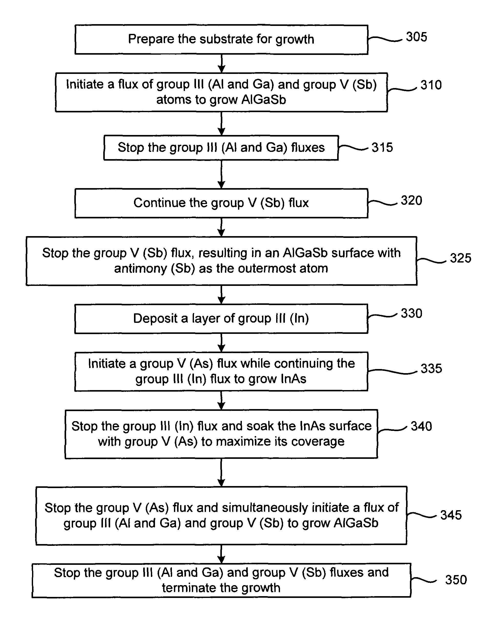
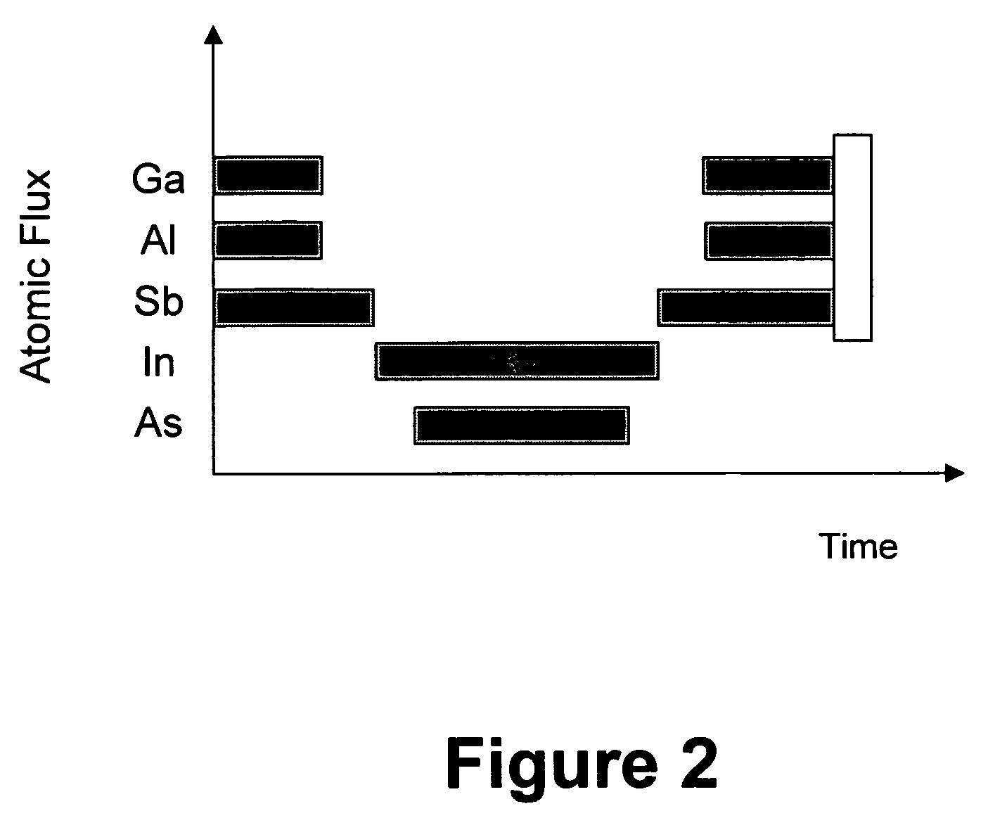
[0024]A method for forming a low defect density heterojunction between a first semiconductor compound (i.e. InAs) and a second semiconductor compound (i.e. AlGaSb). The method controls the sequential deposition of the materials to control the detailed bonding at the heterojunctions, and minimize the nucleation of morphological defects. The method comprises depositing the first semiconductor compound on a substrate by introducing in a deposition chamber a flux of the group III element and the group V element for the first semiconductor compound, covering the deposited first semiconductor compound with a layer of the group V element for the first semiconductor compound to prevent the group III element for the first semiconductor compound from being exposed, and depositing the second semiconductor compound on the layer of the group V element for the first semiconductor compound by introducing in the deposition chamber a flux of the group III element and the group V element for the second semiconductor compound. This may produce an unforced heterojunction between the first and second semiconductor compounds.

Problems solved by technology

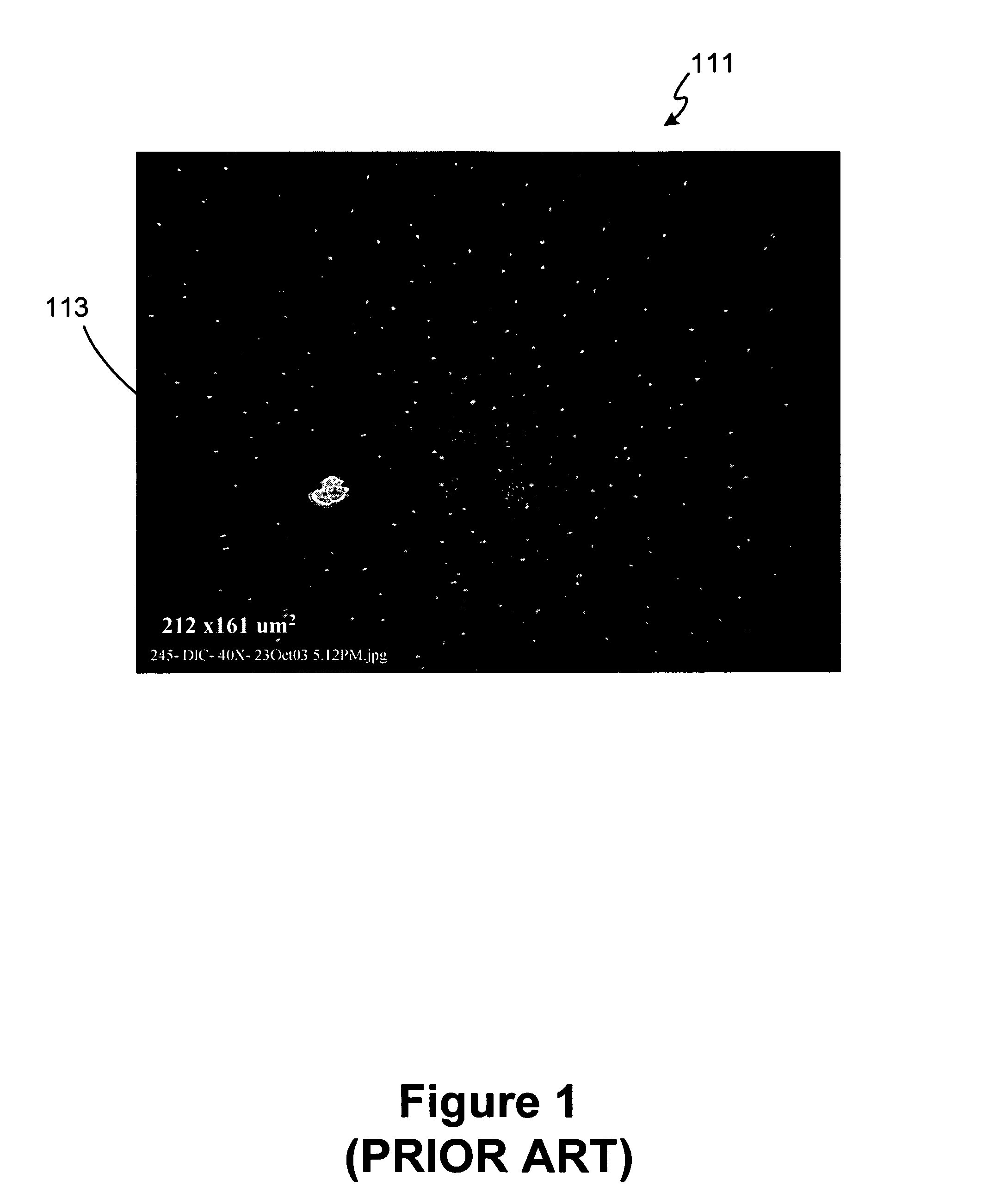
Unfortunately, this procedure causes defects at certain heterojunctions.
If the metal gate crosses one of these defects, excess leakage from the gate to the channel of the transistor occurs.

Method used


Image

  • Process for forming low defect density heterojunctions
  • Process for forming low defect density heterojunctions
  • Process for forming low defect density heterojunctions

Examples


Embodiment Construction

[0026]Methods and systems that implement the embodiments of the various features of the invention will now be described with reference to the drawings. The drawings and the associated descriptions are provided to illustrate embodiments of the invention and not to limit the scope of the invention. Reference in the specification to “one embodiment” or “an embodiment” is intended to indicate that a particular feature, structure, or characteristic described in connection with the embodiment is included in at least an embodiment of the invention. The appearances of the phrase “in one embodiment” or “an embodiment” in various places in the specification are not necessarily all referring to the same embodiment. Throughout the drawings, reference numbers are re-used to indicate correspondence between referenced elements. In addition, the first digit of each reference number indicates the figure in which the element first appears.

[0027]FIG. 1 is a differential interference contrast optical m...


PUM


Abstract

A method for forming a low defect density heterojunction between a first and a second compound, the first and second compounds each includes a group III element combined with a group V element in the periodic table, the method includes the steps of introducing in the deposition chamber the flux of the group III element for the first compound at substantially the same time while introducing in the deposition chamber a flux of the group V element for the second compound, stopping the flux of the group III element for the first compound after a first predetermined time period, stopping the flux of the group V element for the first compound after a second predetermined time period, and introducing in the deposition chamber a flux of the group III element the group V element for the second compound.

Description

[0001]Statement Regarding Government Rights[0002]This invention was made with Government support under contract N66001-01-C-8032 awarded by the Department of Defense, DARPA, US Navy, Space & Naval Warfare Systems (SPAWAR). The Government has certain rights in the invention.BACKGROUND OF THE INVENTION[0003]1. Field of the Invention.[0004]The invention relates generally to a semiconductor fabrication method. More particularly, the invention relates to a process for forming low defect density heterojunctions in semiconductor devices.[0005]2. Description of Related Art.[0006]In advanced semiconductor devices, junctions between two different semiconductor materials are typically used to improve the performance of the device. These junctions, composed of layers of dissimilar semiconductor material, are known in the art as heterojunctions. The semiconductor materials used at the heterojunctions generally have non-equal band gaps and electron affinities.[0007]A heterojunction has two pieces...

Claims


Application Information

Patent Timeline
Patent Type & Authority Patents(United States)
IPC IPC(8): H01L21/3205
CPCH01L21/02463H01L21/02549H01L21/02631H01L29/205H01L29/66446
Inventor SULLIVAN, GERARD J.IKHLASSI, AMALBERGMAN, JOSHUA I.BRAR, BERINDERNAGY, GABOR
Owner TELEDYNE SCI & IMAGING
Learn More