
Active Filler particles in Inks

Inactive Publication Date: 2007-11-15
QINETIQ LTD
View PDF9 Cites 28 Cited by
  • Summary
  • Abstract
  • Description
  • Claims
  • Application Information

AI Technical Summary

Benefits of technology

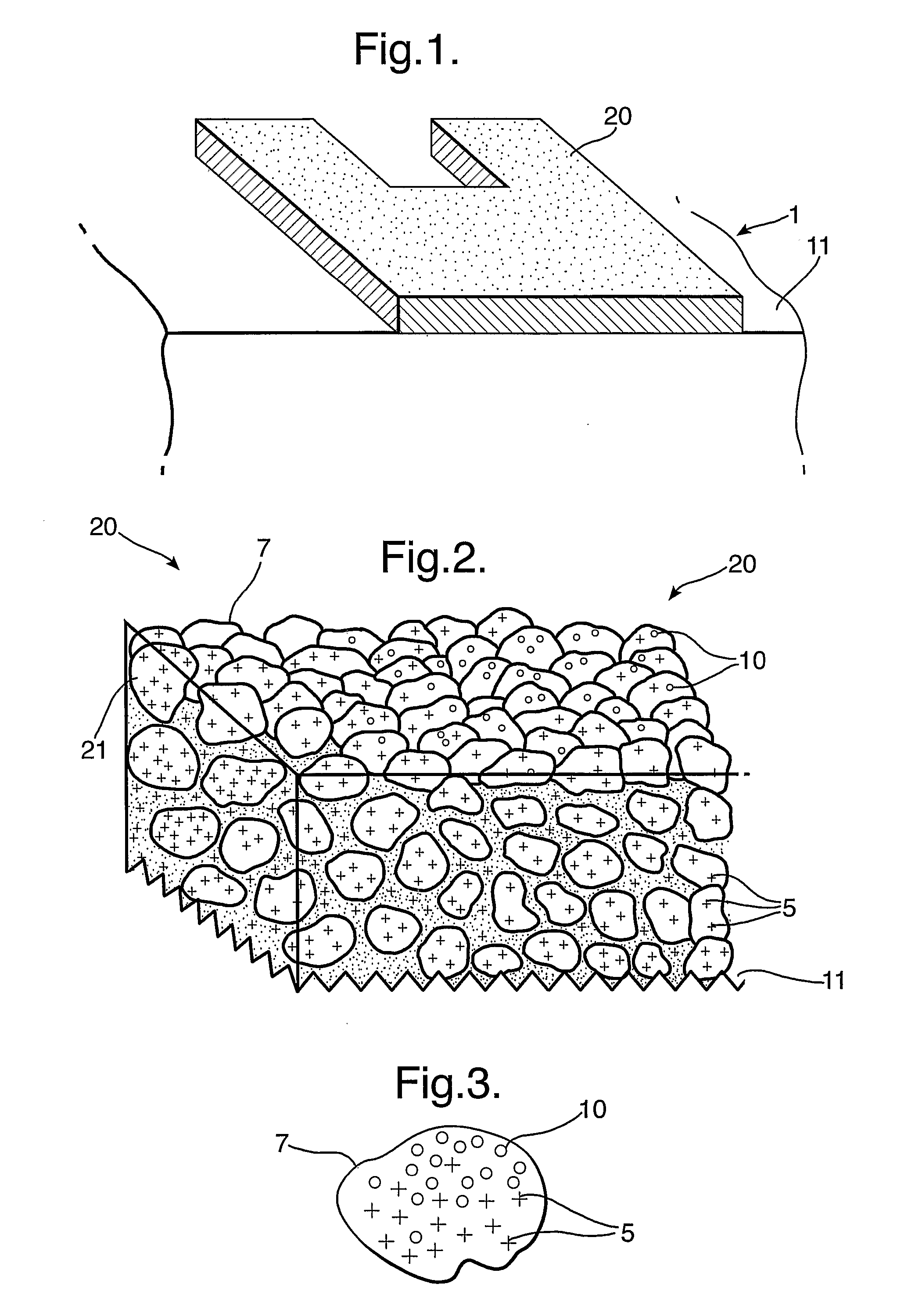
[0038] The electroless solution comprises metal ions, complexing agent(s), reducing agent(s) and may be pH corrected to ensure the electroless deposition reaction occurs between the reducing agent and metal ions on the cured and optionally reduced activating ink composition. The electroless deposition solution is usually heated to increase the reaction rate. For electroless copper or electroless nickel using DMAB reducing agent, the solutions may be conveniently operated at an elevated temperature, ideally in the range 40 to 50° C. The electroless metal deposits only on the portions where the activating ink is deposited and substantially none on the surrounding substrate. The electroless metal continues to deposit onto the activating ink owing to the already deposited electroless metal being autocatalytic to its own electroless deposition. A further advantage of the technology is that the metal can be grown to a controlled thickness, determined by immersion time in the electroless solution. A further advantage of the present invention is the electroless metal deposits onto and / or into the deposited activating ink enabling it to key-in and thus improving the adhesion to the ink and hence substrate.
[0039] The substrate coated with the electroless plate according to the invention, may be further subjected to additional electroless plating solutions and / or conventional electroplating processes, to deposit either an increased thickness of metal and / or to deposit alternative metal(s) to that selected in the original electroless deposition bath, to form a metal plated coating on some or all of the at least one surface of the substrate. Conveniently a further substrate may be formed on and / or applied to the finished or substantially finished metal plated coating and a further process of deposition of ink and electroless metal and / or electrodeposition according to the invention may be carried out, to form a plurality of metal coated substrate layers.
[0040] The substrate may be selected from any material, conveniently such material may include metal or their alloys therein, non-metal, metalloid, conveniently semiconductors, polymer, plastic, fibre or ceramic. The ink may be deposited on at least one side of the substrate. The substrate may be plannar or non-plannar, such as for example a curved surface or a 3-D shape. One convenient substrate would be a rigid or flexible polymer capable of supporting a printed circuit, the polymer may be coated on at least one side, or at least two sides, and optionally the edges and / or through holes.
[0041] The deposited pattern may form an electrical path, such as to provide connection between components on a printed circuit, optionally the deposited pattern may form part or substantially all of an electronic component, which forms part of an electronic circuit.
[0042] Conveniently the width of the deposited material may be controlled by the printing means, ie from the mesh size of a printing means or from repeated passes of the printing means.
[0043] Conveniently the thickness of the metal coating can be controlled by the electroless and / or electrodepostion processes. The thickness of electroless and electrodeposited metals are dependent on the rate of deposition and exposure time to their respective chemistries and heat and in the latter to the supply of electrical power to provide the reduction potential and current flow to the metal depositing at the cathode.

Problems solved by technology

However such metals are expensive and it is desirable to use less expensive metals.
Attempts have been made to use silver as an activation metal, but problems have been found with precipitation due to presence of chloride, daylight or to copper which causes deposition of metallic silver in a non-adherent form.
However it has hitherto not been possible to produce sufficiently uniform and adherent coatings from a silver nitrate activator from an aqueous solution without complexing agents.
Many etch processes used to create porosity in substrates to permit keying-in of electroless metals are hazardous, for example hexavalent chromium solutions with ABS plastics.
However such pastes are expensive and difficult to apply in fine patterns.
A further problem when using a thick paste is that it may affect the subsequent adhesion of the electroless metal and any additional layers including electrodeposited metal layers.
Additionally such high silver loadings pose a risk of leakage from waste sites.

Method used


Image

  • Active Filler particles in Inks
  • Active Filler particles in Inks

Examples


specific examples

Example 1

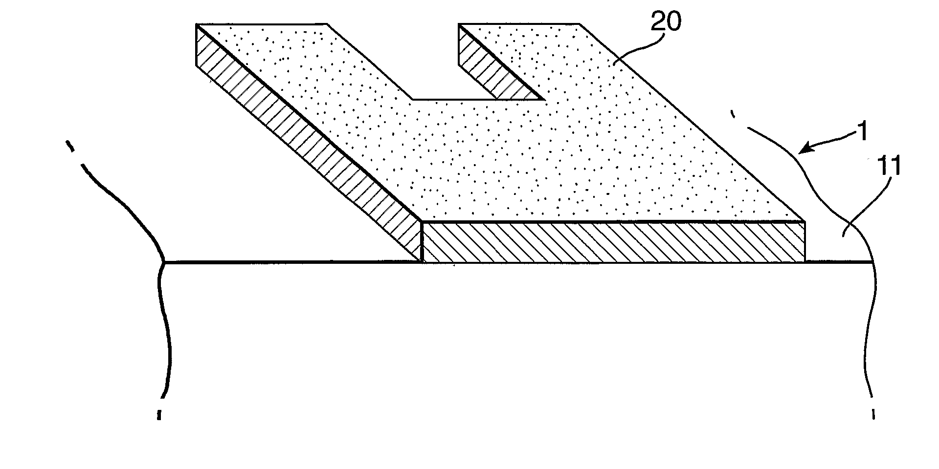
[0058] A screen printing ink (supplied under the trade mark Acheson 6018S) was used as the ink formulation, to which was added titanium dioxide 2 μm at 30% by weight as a filler there was no reducible silver slat present. The control ink composition was screen printed onto two sides of a sheet of polyester in the design of a “Checkpoint®” system electronic article surveillance, (EAS), 1-bit tag.

[0059] The ink was cured by heating the sample to 80° C. for 10 minutes, causing the ink composition to solidify and adhere to the substrate. At this stage the ink had no electrical conductivity. The printed pattern of cured ink was then immersed into a solution of commercially available Enthone 2130® electroless copper at 46° C. as expected there was no electroless deposition of copper metal.

example 2

[0060] A screen printing ink (supplied under the trade mark Acheson 6018S) was used as the ink formulation, to which was added titanium dioxide 2 μm at 30% by weight as a filler and silver nitrate 3% by weight. The silver nitrate was pre-dissolved in an aliquot of ethyl lactate / water to aid the transfer and mixing with the screen printing ink. The activating ink composition was screen printed onto two sides of a sheet of polyester in the design of a “Checkpoint®” system electronic article surveillance, (EAS), 1-bit tag. This tag behaves as an inductively coupling resonator and employs an inductor, L and capacitor, C. A tag of this type can be made to resonate at a selected frequency by changing the design to provide different values of inductance and capacitance.

[0061] The ink was cured by heating the sample to 80° C. for 10 minutes, causing the ink composition to solidify and adhere to the substrate. At this stage the ink had no electrical conductivity. The printed pattern of cure...

example 3

[0062] The same ink used in example 1 was printed and cured into the design of a dipole antenna and also a patch antenna, both commonly employed in UHF RFID tags and other communications devices. The ink composition was cured by heating to 80° C., which when solidified was immersed in the same solution of electroless copper used in example 1. Electroless copper deposited onto the printed ink to a thickness of 2 microns. In this instance the designs did not cause high resistance losses for the thickness of metal and the operating frequency meant that sufficient electromagnetic energy could be absorbed and re-emitted to provide effective devices, without the need for electrodeposited metal.


PUM

PropertyMeasurementUnit
Fractionaaaaaaaaaa
Fractionaaaaaaaaaa
Percent by massaaaaaaaaaa

Abstract

Autocatalytic plating is a form of electrode-less plating in which a metal, for example, cobalt, nickel, gold, silver or copper, is deposited onto a substrate via a chemical reduction process. Coatings derived from this process are usually more uniform and adherent than from other processes and can be applied to unusually shaped surfaces. Non-metallic surfaces can only usually be coated via this process following suitable sensitisation of the substrate. This invention therefore provides a method of preparing a substrate material for subsequent autocatalytic deposition of a metal coating reducing the need for surface preparation by using a reducible silver salt with a suitable filler in a printable ink formulation. Autocatalytic deposition may be used to coat whole surfaces or pre-determined patterns may be deposited by known printing methods.

Description

FIELD OF THE INVENTION [0001] The present invention relates to electroless deposition of metal coatings onto metallic or non-metallic, and especially plastic, substrates. Electroless deposition typically involves reduction of a metal salt in a reducing solution catalysed by an activator or sensitiser deposited on the substrate. BACKGROUND OF THE INVENTION [0002] As described for example in U.S. Pat. No. 4,082,557, electroless deposition typically involves four steps: [0003] 1 Mordanting in which the articles to be metal coated are treated with acids, typically chromic and / or sulphuric acids, to render the surface wettable and microporous; [0004] 2 Sensitisation in which the mordanted surface is treated with stannous chloride and hydrochloric acid to deposit stannous chloride in the pores; [0005] 3 Activation in which the surfaces are immersed in a solution of a salt of a noble metal so that small quantities of noble metal are attached to the surface; and [0006] 4 Metal coating in wh...

Claims


Application Information

Patent Timeline
IPC IPC(8): C09D11/00B05D3/10C09D11/10C23C18/16C23C18/20C23C18/31H05K3/18
CPCC09D11/101C23C18/1608C23C18/1653C23C18/1831H05K2203/0709C23C18/31H05K3/182H05K2201/0209H05K2201/0212C23C18/30
Inventor JOHNSON, DANIEL R.WILLIS, RICHARD L.DAMERALL, WILLIAM N.
Owner QINETIQ LTD
Learn More