
Composite substrate and method of fabricating the same

a composite substrate and substrate technology, applied in the direction of basic electric elements, electrical apparatus, semiconductor devices, etc., can solve the problems of difficult production of composite substrates containing a very thin buried insulating layer, fga treatment is relatively ineffective at each interface encountered, and the effect of improving electrical properties

Active Publication Date: 2007-07-26
S O I TEC SILICON ON INSULATOR THECHNOLOGIES
View PDF13 Cites 21 Cited by
  • Summary
  • Abstract
  • Description
  • Claims
  • Application Information

AI Technical Summary

Benefits of technology

[0018]The present invention improves the mobility of holes and / or electrons in the active layer. As an illustrative example, it is desirable and possible to obtain an electron mobility of more than 500 centimetervolt−1·second−1 (cm2·V−1·s−1) in silicon doped with boron in a concentration of the order of 1015 atoms / cm3 with the present invention.
[0020]The remainder of the description focuses on the DIT value, as it is one of the principal parameters on which the substrate formation steps of the present invention have an influence. Further, the DIT parameter has an effect on electron mobility. The present invention improves the electrical performances of the final composite substrate.
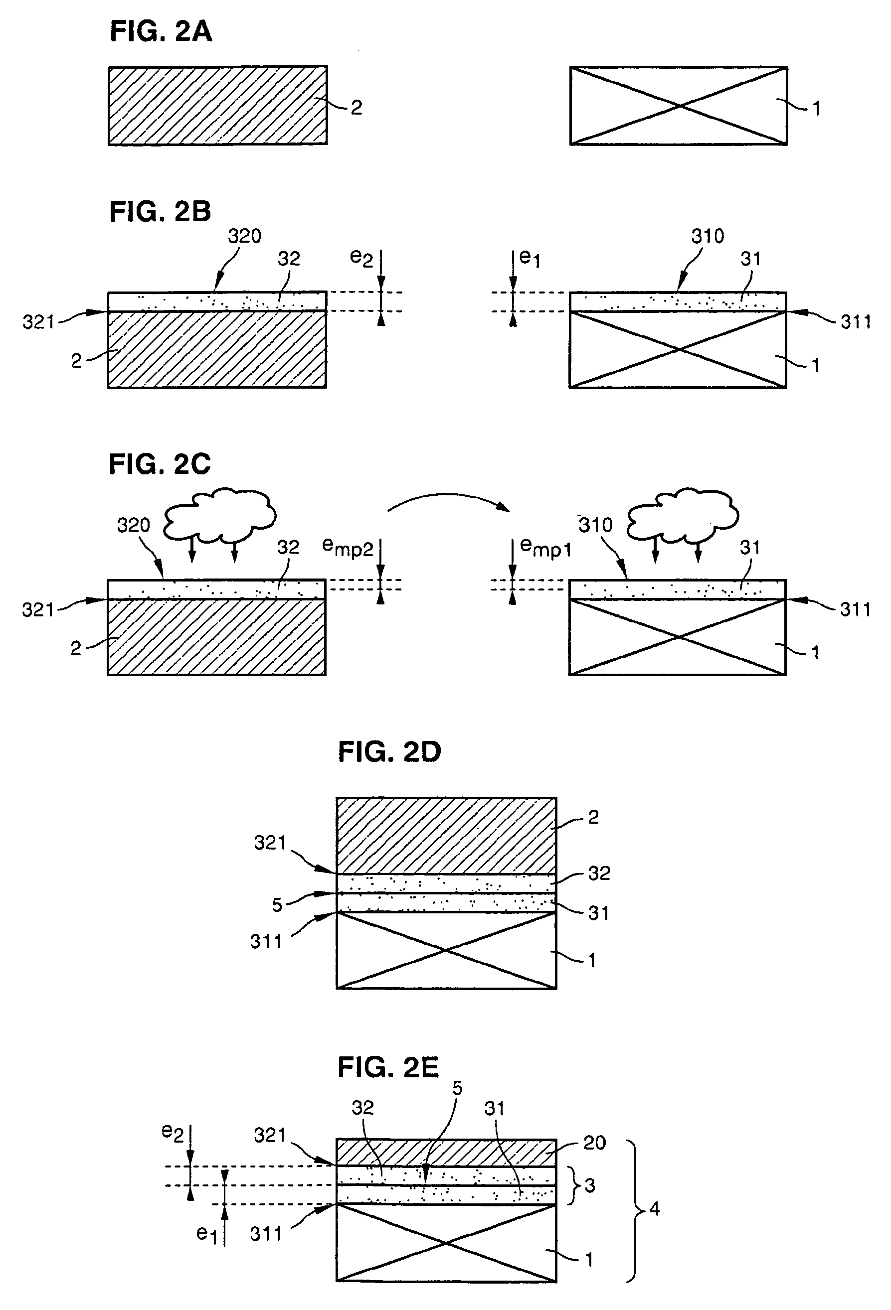
[0032]The method can further provide for thinning at least one of the first and second insulating layers, after plasma activation and prior to bonding.

Problems solved by technology

The FGA treatment method loses effectiveness at each interface that is encountered.
Thus, the FGA treatment is relatively ineffective for deep-lying interfaces.
It is well known that producing composite substrates comprising a very thin buried insulating layer is difficult.

Method used


Image

  • Composite substrate and method of fabricating the same
  • Composite substrate and method of fabricating the same
  • Composite substrate and method of fabricating the same

Examples


example 1

Preparation of an SOI Type Substrate with an Oxide Laver Thickness of 25 nm

[0116]Thermal oxidation of a 200 mm diameter silicon substrate was carried out to form a 10 nm thick insulating layer of silicon oxide (SiO2) thereon. In a similar manner, a 15 nm thick silicon oxide layer was formed on a silicon source substrate of the same size. Next, the two substrates underwent FGA heat treatment to arrive at the electrical properties of the two oxides.

[0117]The silicon source substrate then underwent a hydrogen ion implantation step, carried out through the silicon oxide layer covering it. Implantation was carried out at a dose of 5.5×10¹⁶ H+ / cm2 using an implantation energy of 35 keV.

[0118]Next, the upper surface of the substrate was cleaned with a SC1 solution then with SC2 in succession.

[0119]The silicon oxide layer of the source substrate thus prepared then underwent an oxygen plasma activation treatment applied for 30 seconds at a power density of 0.8 W / cm2, at an oxygen pressure of...

example 2

Preparation of an SOI Type Substrate with an Oxide Thickness of 11 nm

[0127]The procedure of Example 1 was used, respectively with oxide thicknesses of 3 nm on the support substrate and 10 nm on the source substrate. The oxides obtained were then treated at 450° C. for about 1 hour in an atmosphere formed by 2% hydrogen in argon (FGA treatment) to improve the DIT values.

[0128]The source substrate, which comprised the thickest oxide layer, was activated by plasma at a power of 2 W / cm2, resulting in a modification of the oxide over about 7 nm.

[0129]This plasma treated insulating layer was cleaned in a SC1 solution using a concentration, temperature and time sufficient to etch it over a depth of the order of 2 nm. The final composite substrate obtained was an SOI type structure which comprised a buried insulating layer with a thickness on the order of 11 nm and which had good electrical qualities, in particular a DIT of the order of several 1010·eV−1·cm−2.

example 3

Preparation of a GeOI Type Substrate with an Oxide Thickness of 20 nm

[0130]A 5 nm layer of HfO2 was formed on a 200 mm diameter source substrate of bulk germanium. In a variation, the source substrate may consist of a 200 mm silicon wafer on which a layer of germanium has been formed by epitaxy.

[0131]A 15 nm layer of silicon oxide (SiO2) was formed on a silicon (Si) support substrate.

[0132]The silicon oxide layer of the support substrate then underwent an oxygen plasma activation treatment applied for 30 seconds with a power density of 0.4 W / cm2 at an oxygen pressure of 50 mTorr (6.66 Pa), with a flow rate of 75 sccm, at 20° C.

[0133]Bonding was then carried out followed by lifting off the upper portion of the germanium source substrate by detachment using the SmartCut™ method. A GeOI substrate was obtained with a DIT value of the order of several 1011·eV−1·cm−2 at the interface with the germanium and several 1010·eV−1·cm−2 at the interface with the silicon.

[0134]It should be noted t...


PUM


Abstract

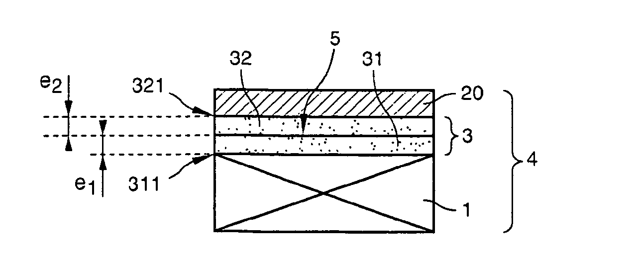
The invention specifically relates to methods of fabricating a composite substrate by providing a first insulating layer on a support substrate at a thickness of e1 and providing a second insulating layer on a source substrate at a thickness of e2, with each layer having an exposed face for bonding; providing plasma activation energy in an amount sufficient to activate a portion of the thickness of the face of the first insulating layer emp1 and a portion of the thickness of the face of the second insulating layer emp1; providing a final insulating layer by molecular bonding the activated face of the first insulating layer with the activated face of the second insulating layer; and removing a back portion of the source substrate while retaining an active layer comprising a remaining portion of the source substrate bonded to the support substrate with the final insulating layer interposed therein to form the composite substrate. The thicknesses e1, e2 of the first and second insulating layers are sufficient to provide the final insulating layer with a thickness of 50 nanometers or less, and the plasma activation energy and respective thicknesses e1, e2 of the first and second insulating layers are selected such that only respective thicknesses emp1 and emp2 of the faces of the first insulating layer and the second insulating layer are activated.

Description

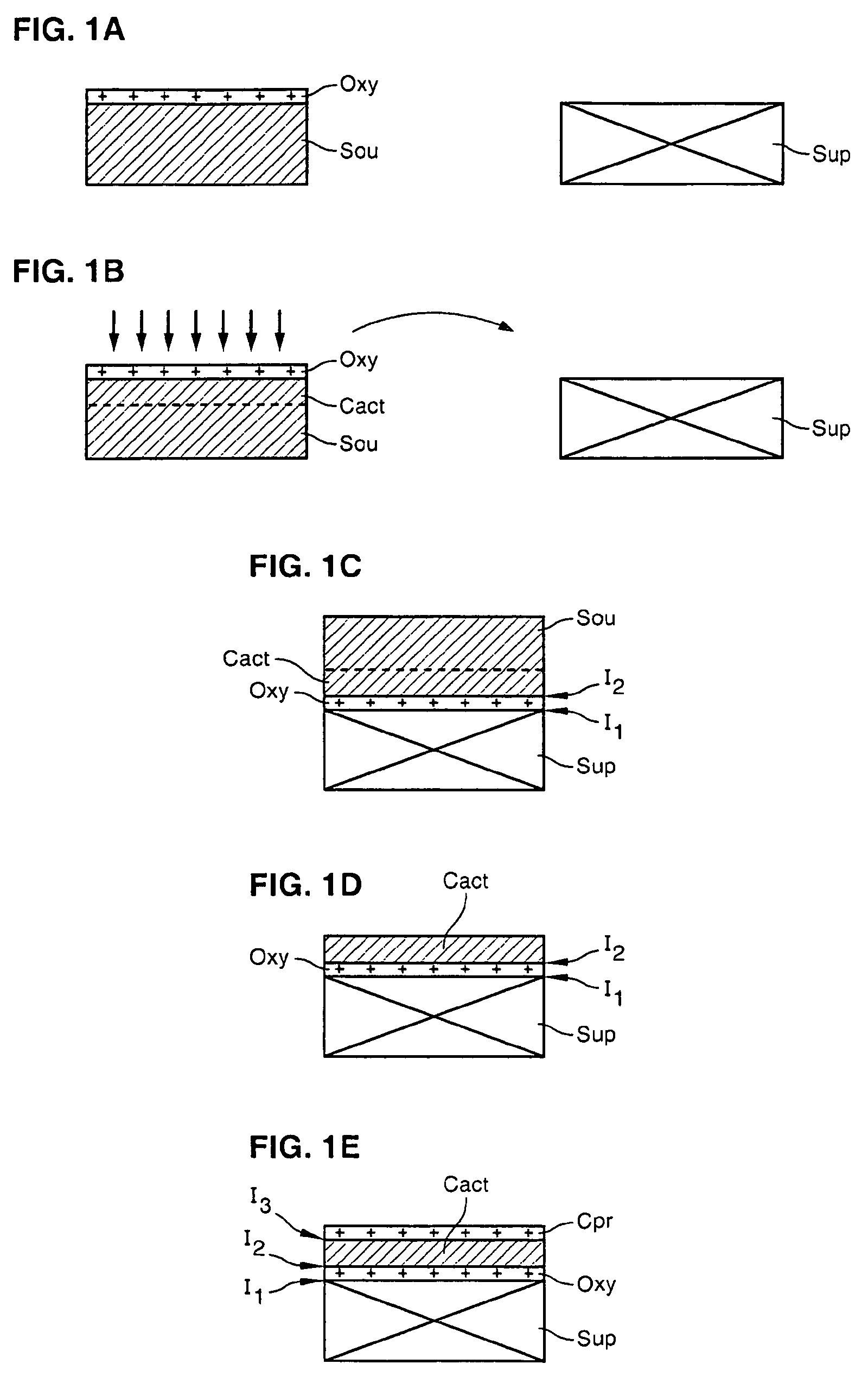
TECHNICAL FIELD[0001]The present invention relates to a method of fabricating a composite substrate comprising an insulating layer that is buried. The insulating layer is, for example, interposed between a semiconductor support substrate and an active layer of semiconductor material.[0002]More precisely, the present invention relate to a method of obtaining a composite substrate, wherein the insulating layer is thin, for example, less than 50 nanometers (nm) thick, or even less than 20 nm thick, with substantially improved electrical properties. Such a substrate can be used in particular in the fields of optics, electronics, and optoelectronics.[0003]A particular but non-limiting example of that type of composite substrate is a substrate known by its acronym Silicon On Insulator (SOI), which designates a substrate comprising a layer of insulating silicon oxide interposed between two layers of silicon.BACKGROUND ART[0004]FIGS. 1A to 1E illustrate the various steps of one mode of fabr...

Claims


Application Information

Patent Timeline
Patent Type & Authority Applications(United States)
IPC IPC(8): H01L27/12H01L21/84
CPCH01L21/76251H01L21/20
Inventor ALLIBERT, FREDERICKERDILES, SEBASTIEN
Owner S O I TEC SILICON ON INSULATOR THECHNOLOGIES
Learn More