LOCOS-based Schottky barrier diode and its manufacturing methods

a technology of schottky barrier diodes and manufacturing methods, which is applied in the direction of basic electric elements, electrical apparatus, and semiconductor devices, can solve the problems of poor step coverage of patterned metal layers, difficulty in simultaneously obtaining a higher reverse breakdown voltage and a lower forward voltage (vsub>f/sub>), and achieve the reduction of junction curvature effect, reduce parasitic series resistance, and reduce reverse leakage current

Inactive Publication Date: 2006-06-01
SILICON BASED TECH
View PDF4 Cites 15 Cited by
  • Summary
  • Abstract
  • Description
  • Claims
  • Application Information

AI Technical Summary

Benefits of technology

[0010] The present invention discloses a LOCOS-based Schottky barrier diode and its manufacturing methods. The LOCOS-based Schottky barrier diode of the present invention comprises a semiconductor substrate of a first conductivity type being comprised of a lightly-doped epitaxial silicon layer formed on a heavily-doped silicon substrate, a raised diffusion guard ring of a second conductivity type being formed between an outer LOCOS field oxide layer and an inner LOCOS field oxide layer, a recessed semiconductor substrate with or without a compensated diffusion layer being surrounded by the raised diffusion guard ring, a metal silicide layer being formed over a semiconductor surface including a portion of the raised diffusion guard ring and the recessed semiconductor substrate surrounded by the raised diffusion guard ring, and a patterned metal layer being at least formed over the metal silicide layer, wherein the...

Problems solved by technology

As a consequence, it is difficult to simultaneously obtain a higher reverse breakdown voltage and a lower forward volt...

Method used


Image

  • LOCOS-based Schottky barrier diode and its manufacturing methods
  • LOCOS-based Schottky barrier diode and its manufacturing methods
  • LOCOS-based Schottky barrier diode and its manufacturing methods

Examples


Embodiment Construction

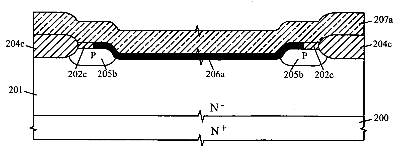
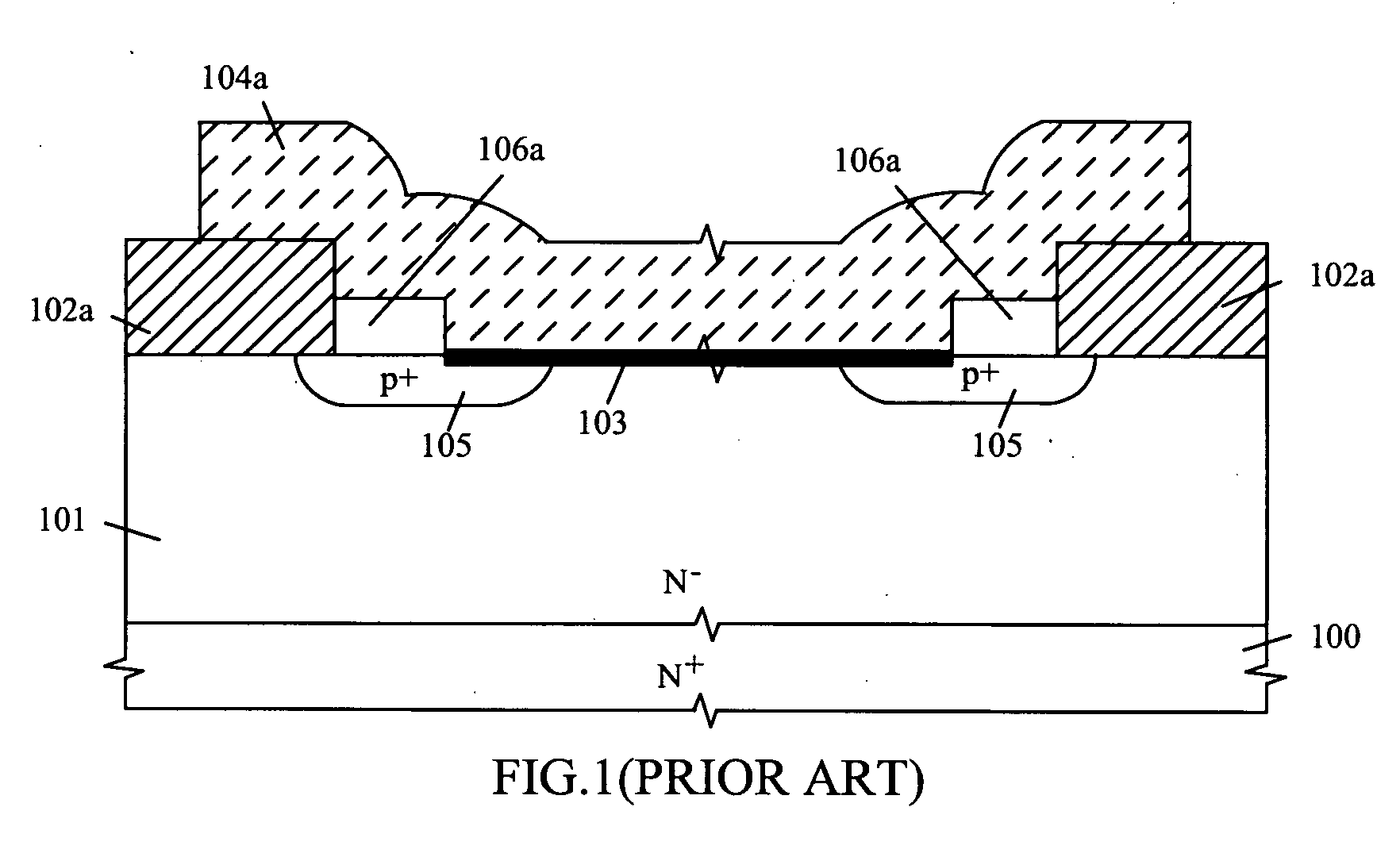
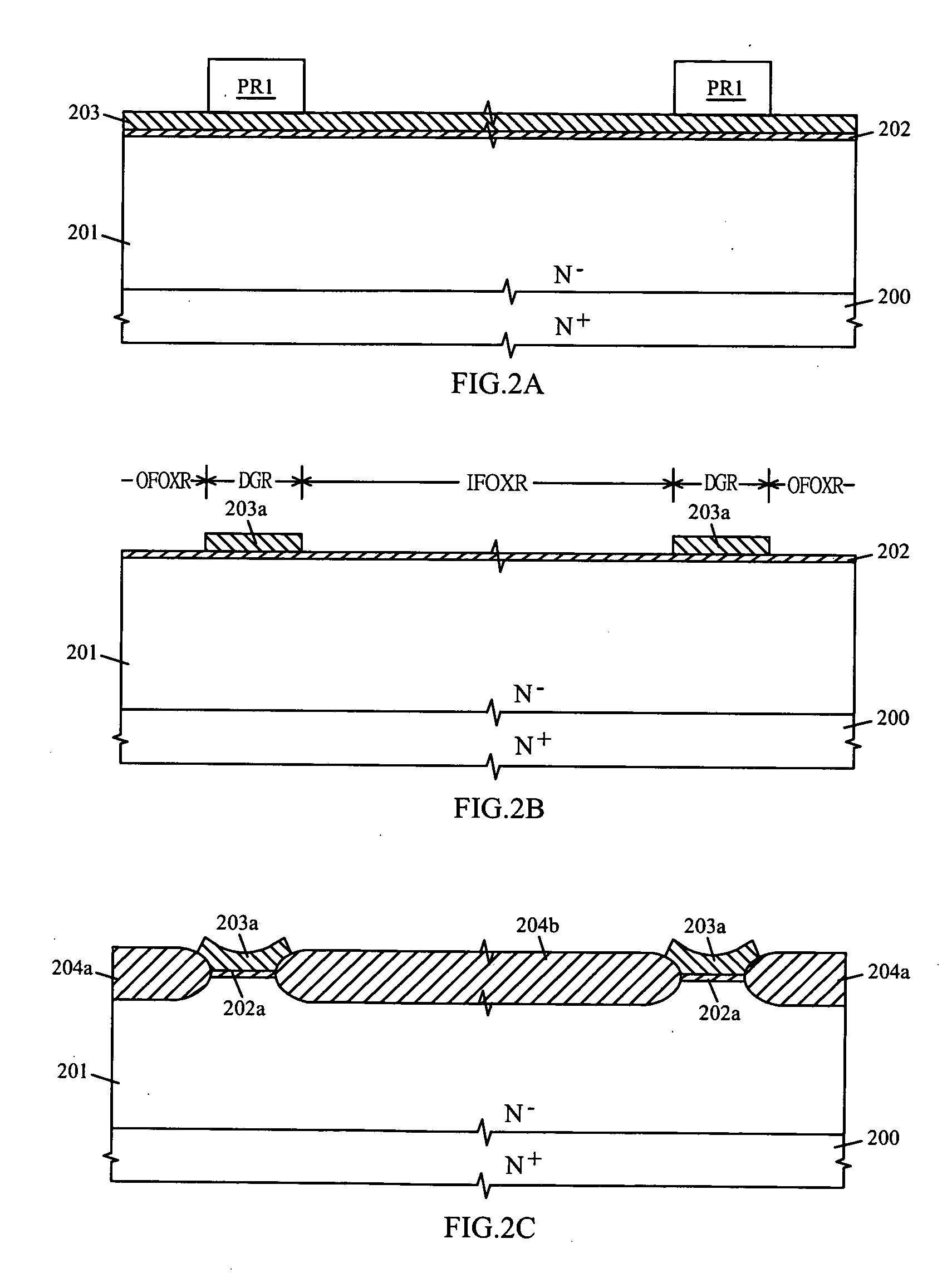
[0016] Referring now to FIG. 2A through FIG. 2G, there are shown process steps and their schematic cross-sectional views of fabricating a first-type LOCOS-based Schottky barrier diode of the present invention.

[0017]FIG. 2A shows that a pad oxide layer 202 is formed on a semiconductor substrate 201 / 200 of a first conductivity type; a masking silicon nitride layer 203 is then formed on the pad oxide layer 202; and subsequently, a first masking photoresist (PR1) step is performed to define a diffusion guard ring region (DGR). The pad oxide layer 202 is a thermal silicon dioxide layer grown on the semiconductor substrate 201 / 200 in a dry oxygen ambient and its thickness is preferably between 100 Angstroms and 500 Angstroms. The masking silicon nitride layer 203 is formed by low-pressure chemical vapor deposition (LPCVD) and its thickness is preferably between 500 Angstroms and 1500 Angstroms. The semiconductor substrate 201 / 200 comprises a lightly-doped epitaxial silicon layer 201 bein...


PUM


Abstract

The LOCOS-based Schottky barrier diode of the present invention comprises a raised diffusion guard ring surrounded by an outer LOCOS field oxide layer, a recessed semiconductor substrate with or without a compensated diffusion layer surrounded by the raised diffusion guard ring, a metal silicide layer formed over a portion of the raised diffusion guard ring and the recessed semiconductor substrate, and a patterned metal layer formed at least over the metal silicide layer, wherein the raised diffusion guard ring is formed between an inner LOCOS field oxide layer and the outer LOCOS field oxide layer and the recessed semiconductor substrate is formed by removing the inner LOCOS field oxide layer. The LOCOS-based Schottky barrier diode comprises the raised diffusion guard ring to reduce junction curvature effect on reverse breakdown voltage, the recessed semiconductor substrate to reduce forward voltage, and the compensated diffusion layer to reduce reverse leakage current.

Description

BACKGROUND OF THE INVENTION [0001] 1. Field of the Invention [0002] The present invention relates generally to a Schottky barrier diode and its manufacturing method and, more particularly, to a LOCOS-based Schottky barrier diode (LBSBD) and its manufacturing methods. [0003] 2. Description of the Related Art [0004] A Schottky barrier diode comprising a metal-semiconductor contact is known to be a majority-carrier device and is therefore used as a high-speed switching diode or a high-frequency rectifier. For a Schottky barrier diode used as a power switching diode, the major design issues are concentrated on reverse breakdown voltage (VB), reverse leakage current (IR), forward current (If) and forward voltage (Vf). In general, a diffusion guard ring is required to reduce the reverse leakage current due to edge effect of the metal-semiconductor contact and to relax soft breakdown due to high edge field. However, the diffusion guard ring may produce junction curvature effect on the reve...

Claims


Application Information

Patent Timeline
IPC IPC(8): H01L29/47
CPCH01L29/66143H01L29/872
Inventor WU, CHING-YUAN
Owner SILICON BASED TECH
Why Eureka
Try Eureka