soi transistor and manufacturing method thereof

A manufacturing method and transistor technology, applied in semiconductor/solid-state device manufacturing, semiconductor devices, electrical components, etc., can solve the problem of large parasitic series resistance, reduce parasitic series resistance, improve reliability, and avoid leakage current.

Active Publication Date: 2014-10-22
SEMICON MFG INT (SHANGHAI) CORP
View PDF8 Cites 0 Cited by
  • Summary
  • Abstract
  • Description
  • Claims
  • Application Information

AI Technical Summary

Problems solved by technology

[0005] The object of the present invention is to provide a kind of SOI transistor and its manufacturing method, to solve the problem that the parasitic series resistance of existing SOI transistor source-drain region and source-drain extension region is large

Method used


Image

  • soi transistor and manufacturing method thereof
  • soi transistor and manufacturing method thereof
  • soi transistor and manufacturing method thereof

Examples


Embodiment Construction

[0022] The SOI transistor and its manufacturing method proposed by the present invention will be further described in detail below with reference to the accompanying drawings and specific embodiments. Advantages and features of the present invention will be apparent from the following description and claims. It should be noted that all the drawings are in a very simplified form and use imprecise scales, and are only used to facilitate and clearly assist the purpose of illustrating the embodiments of the present invention.

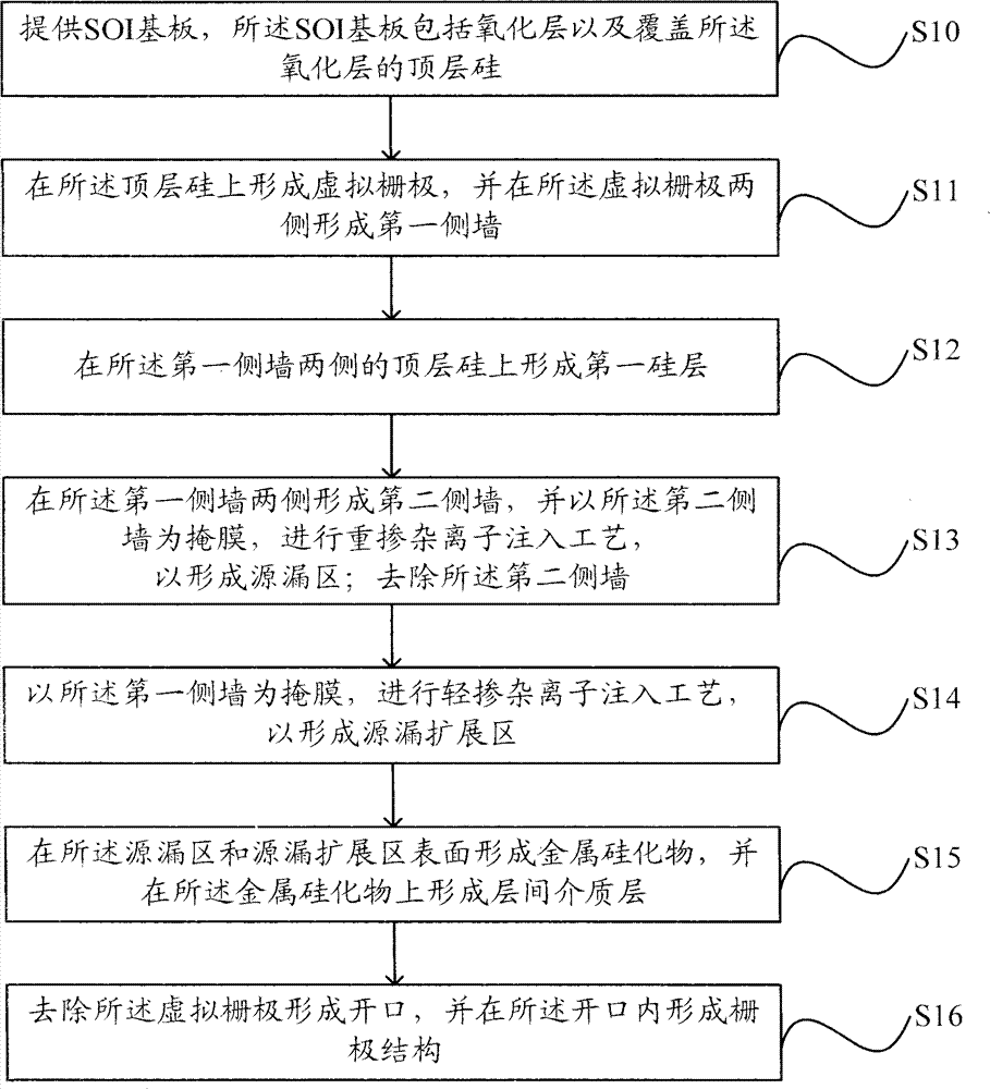
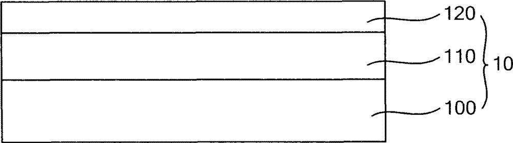
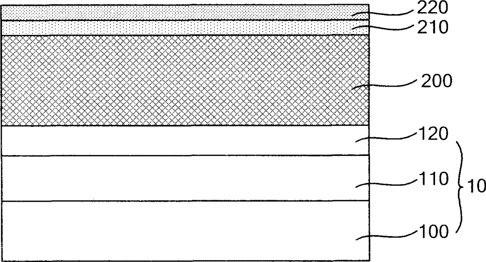
[0023] Please refer to figure 1 and Figure 2a ~2g, of which, figure 1 It is a flowchart of a method for manufacturing an SOI transistor according to an embodiment of the present invention; Figure 2a ˜2g is a schematic diagram of a method for manufacturing an SOI transistor according to an embodiment of the present invention. The manufacturing method of the SOI transistor provided by the embodiment of the present invention includes the following steps:...


PUM

PropertyMeasurementUnit
thicknessaaaaaaaaaa
thicknessaaaaaaaaaa
thicknessaaaaaaaaaa

Abstract

The invention provides an SOI (silicon on insulator) transistor and a manufacture method of the SOI transistor. The manufacture method comprises the following steps of: providing an SOI base plate, wherein the SOI base plate comprises an oxidation layer and top-layer silicon covering the oxidation layer; forming a virtual grid electrode on the top-layer silicon, and forming a first side wall at two sides of the virtual grid electrode respectively; forming a first silicon layer on the top-layer silicon at two sides of the first side wall respectively; forming a second side wall at two sides of each first side wall respectively, and with the second side wall as masks, carrying out a heavy doping ion implantation technology to form a source / drain region; removing the second side walls; with the first side walls as masks, carrying out a light doping ion implantation technology to form a source / drain expanding region; forming metal silicide on the surfaces of the source / drain region and the source / drain expanding region, and forming an interlayer medium layer on the metal silicide; and removing the virtual grid electrode to form an opening, and forming a grid electrode in the opening. According to the SOI transistor and the manufacture method of the SOI transistor provided by the invention, the parasitic series resistance of the source / drain region and the source / drain expanding region of the SOI transistor can be reduced.

Description

technical field [0001] The invention relates to an integrated circuit manufacturing process, in particular to an SOI transistor and a manufacturing method thereof. Background technique [0002] The main device in an integrated circuit, especially a VLSI, is a metal oxide semiconductor field effect transistor (MOSFET for short). Since the MOSFET was invented, its geometric size has been continuously reduced, and its feature size is now in the sub-tenth of a micron region. In this region, various practical and fundamental constraints begin to appear, and further scaling down of device dimensions is becoming more and more difficult. As far as conventional complementary metal-oxide-semiconductor (complementary metal oxide semiconductor, referred to as CMOS) integrated circuit technology is concerned, with the continuous reduction of the feature size of MOS devices, in order to suppress the short channel effect, the geometric dimensions of other parts are also reduced. must be ...

Claims


Application Information

Patent Timeline
Patent Type & Authority Patents(China)
IPC IPC(8): H01L21/762H01L21/28H01L21/336H01L21/265H01L29/06H01L29/40H01L29/78
Inventor 刘金华
Owner SEMICON MFG INT (SHANGHAI) CORP
Why Eureka
Try Eureka