Semiconductor device and manufacturing method thereof

A manufacturing method and semiconductor technology, applied in the fields of semiconductor/solid-state device manufacturing, semiconductor devices, electrical components, etc., can solve the problems of easy agglomeration, silicide films cannot withstand high temperature annealing, and poor thermal stability of silicide films, etc.

Active Publication Date: 2015-09-23
INST OF MICROELECTRONICS CHINESE ACAD OF SCI
View PDF5 Cites 0 Cited by
  • Summary
  • Abstract
  • Description
  • Claims
  • Application Information

AI Technical Summary

Problems solved by technology

However, as the thickness of metal silicide sources and drains becomes thinner, its thermal stability will also deteriorate
like image 3 As shown, after the size is reduced, the channel 20 / 21 becomes shorter, and the metal silicide source-drain film 30 / 31 must be correspondingly thinned in order to better control the short channel effect, but the thinned silicide film 30 / 31 is The thermal stability is poor during annealing, and it is easy to agglomerate, resulting in a sharp increase in resistivity
Since in the aforementioned SADS method for reducing SBH, the silicide film cannot withstand the high-temperature annealing required to separate and condense the dopant ions at the silicide / silicon interface, therefore, for the metal silicide source-drain MOSFET, it cannot be reduced SBH
[0010] All in all, metal silicide source-drain MOSFET is regarded as the structure of sub-20nm next-generation CMOS, and the existing SADS method in order to reduce the SBH between the source and channel regions to improve the driving ability, shortens the channel, metal silicide It cannot be implemented because it cannot withstand high temperature annealing when the film is thinned

Method used


Image

  • Semiconductor device and manufacturing method thereof
  • Semiconductor device and manufacturing method thereof
  • Semiconductor device and manufacturing method thereof

Examples


Embodiment Construction

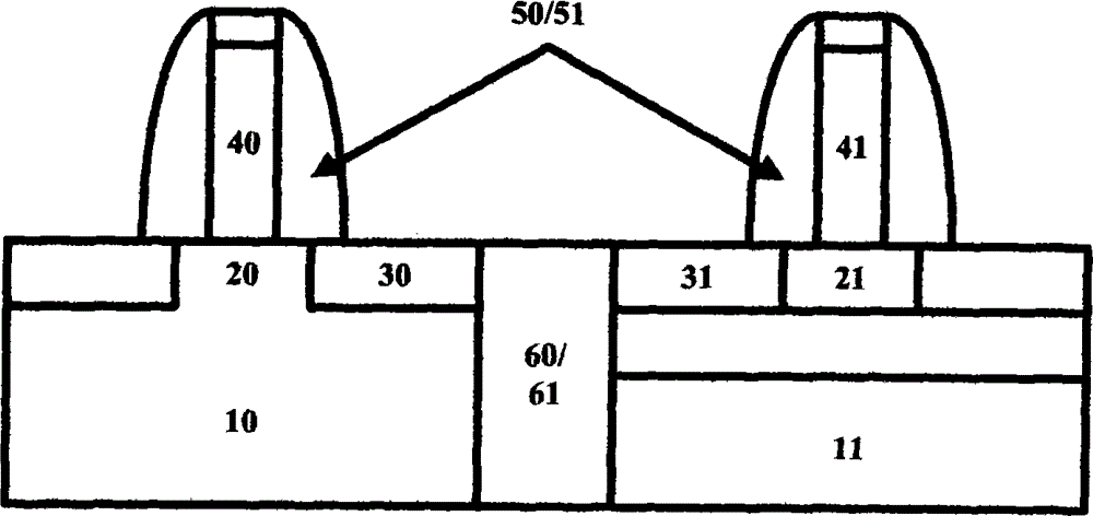
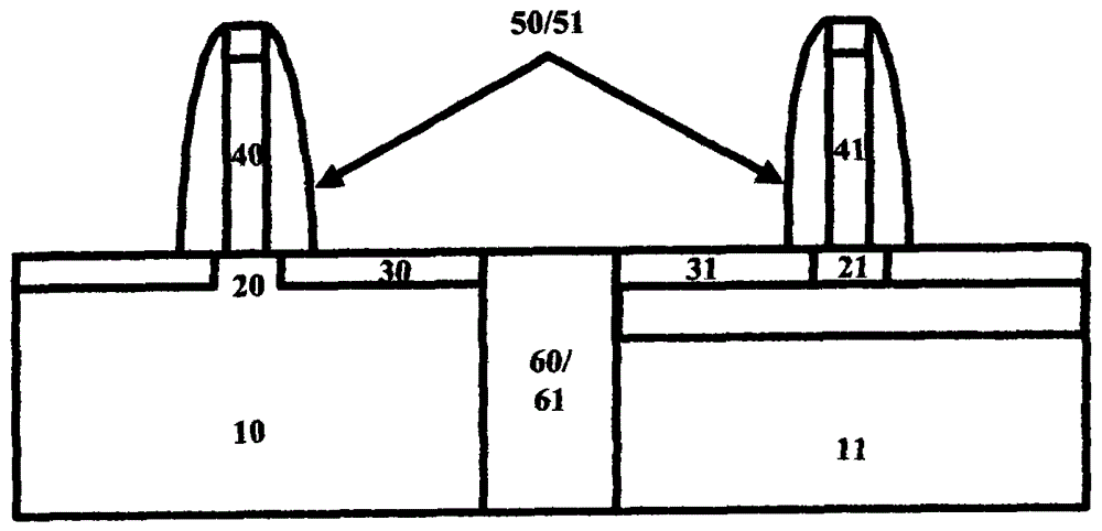
[0033] The features and technical effects of the technical solution of the present invention will be described in detail below with reference to the accompanying drawings and in conjunction with schematic embodiments, and a MOSFET with thermally stable epitaxially grown ultra-thin metal silicide source and drain and its manufacturing method are disclosed. It should be pointed out that similar reference numerals represent similar structures, and the terms "first", "second", "upper", "lower" and the like used in this application can be used to modify various device structures. These modifications do not imply a spatial, sequential or hierarchical relationship of the modified device structures unless specifically stated.

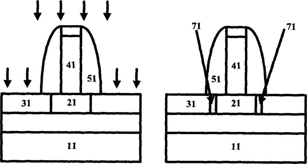
[0034] Figure 4 to Figure 8It is a device cross-sectional diagram corresponding to each step of the method for manufacturing an epitaxially grown ultra-thin metal silicide source-drain MOSFET according to the present invention. In each figure, the STI is not ...


PUM


Abstract

A semiconductor device includes substrates (100, 110), channel regions (200, 210) in the substrates (100, 110), source and drain regions (700, 710) on both sides of the channel regions (200, 210), gate structures (300, 310) on the channel regions (200, 210), and gate sidewalls (400, 410) around the gate structures (300, 310). The source and drain regions (700, 710) are made of epitaxial ultra thin metal silicide. Dopant ions segregation regions (800, 810) are formed at the interface between the source and drain regions (700, 710) and the channel regions (200, 210). The semiconductor device and manufacturing method thereof can reduce Schottky barrier height of metal oxide semiconductor field effect transistor with short channel and epitaxial ultra thin metal silicide source and drain, so as to improve device driving performance.

Description

technical field [0001] The present application relates to a semiconductor device and a manufacturing method thereof, in particular to a MOSFET structure with an epitaxially grown ultra-thin metal silicide source / drain and a manufacturing method thereof. Background technique [0002] The current IT application field continuously requires IC integration to be greatly improved. As traditional MOSFET devices continue to be scaled down, some parameters that can be controlled in the process, such as channel length, gate oxide thickness, substrate doping concentration, etc., can be changed proportionally. , although the impact of process fluctuations is greater as the device size decreases, many physical parameters such as silicon band gap, Fermi potential, interface state and oxide layer charge, thermoelectric potential and pn junction self-built potential, etc. cannot be scaled changes, which greatly affect the performance of scaled-down devices. [0003] One of these is the sou...

Claims


Application Information

Patent Timeline
Patent Type & Authority Patents(China)
IPC IPC(8): H01L29/78H01L29/06H01L21/336H01L21/324
CPCH01L29/78618H01L29/7839H01L21/26506H01L29/66643H01L29/66772H01L29/47H01L21/26513
Inventor 罗军赵超
Owner INST OF MICROELECTRONICS CHINESE ACAD OF SCI
Why Eureka
Try Eureka