Magnetic element and magnetic element array
a magnetic element and array technology, applied in the field of magnetic element and magnetic element array, can solve the problems of high current requirement, difficult to simply combine a direct-current-driving type magnetic element with a conventional magnetoresistance effect element which may have a far larger resistance, and achieve low writing current, the effect of increasing the output level of the reproducing signal
- Summary
- Abstract
- Description
- Claims
- Application Information
AI Technical Summary
Benefits of technology
Problems solved by technology
Method used
Image
Examples
examples
[0146] Hereafter, embodiments of the invention will be explained in greater detail in conjunction with examples.
first example
[0147] First, a magnetic element of the first embodiment was manufactured as the first example of the invention.
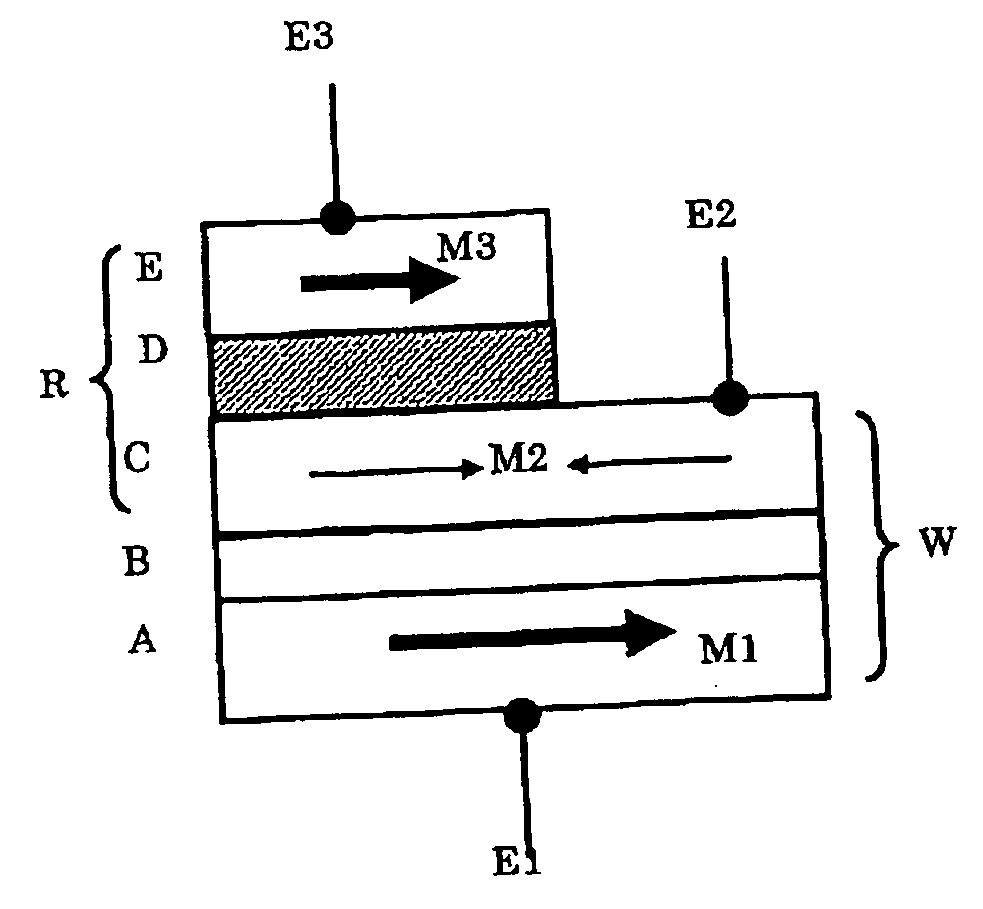
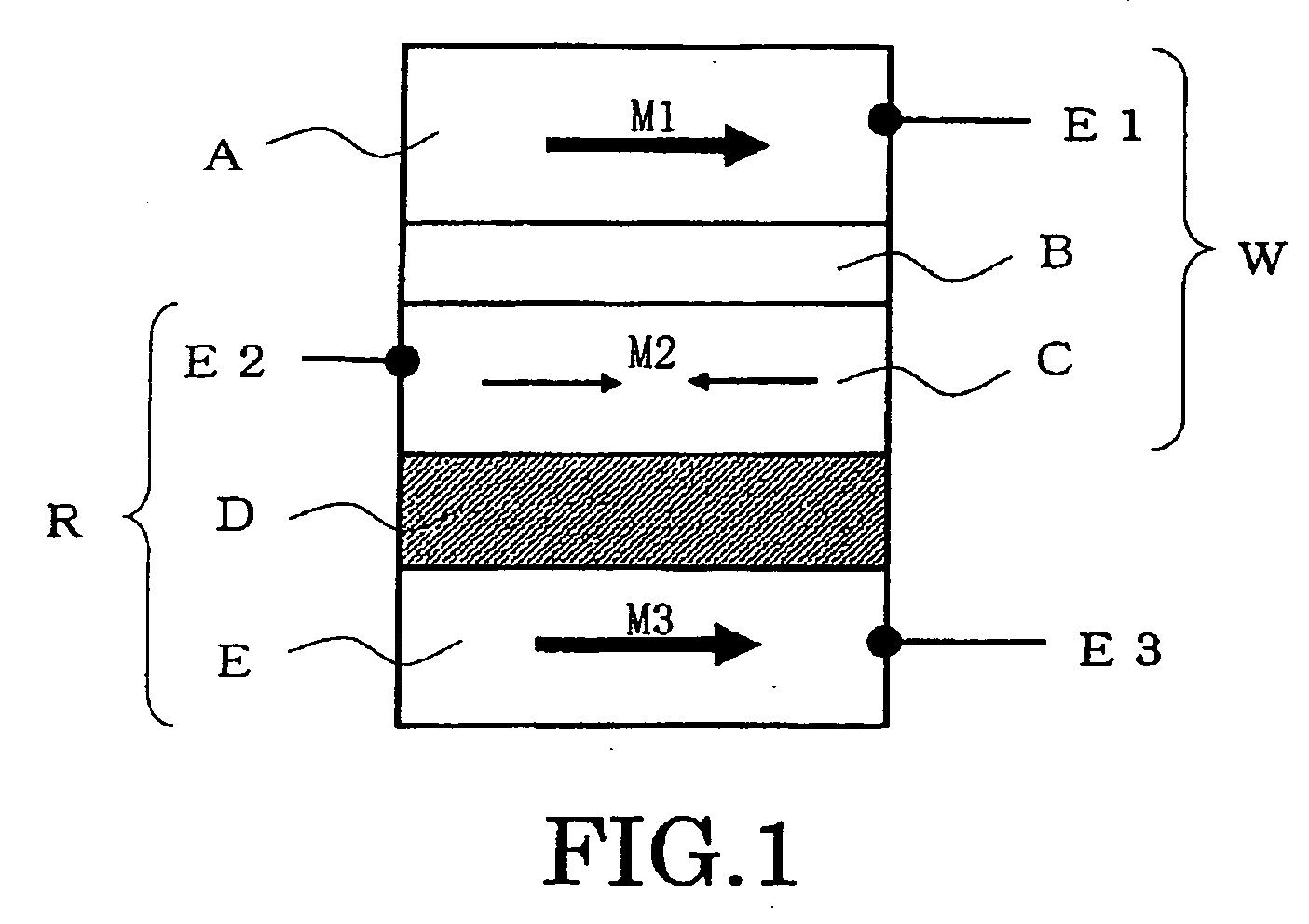
[0148]FIGS. 17A and 17B are schematic diagrams showing a principal part sectional structures of a magnetic elements of the example.
[0149] These laminated structures were produced using ultra-high vacuum sputtering equipment.
[0150] First, FETs were formed by a usual CMOS process on a Si wafer as a substrate. The bottom electrode film (not shown) which consists of tantalum (Ta) and copper (Cu) was formed on the substrate. Furthermore, the laminated structure which included the same elements as shown in FIGS. 17A and 17B were formed in a order of upside down to the figures and the upper electrode layer was formed on it. EB (electron beam) resist was applied on this laminated structure, EB exposure process was performed, and the laminated film was processed into 60 nm×240 nm size by using a lift-off process. Furthermore, EB drawing process and lift-off process were performe...
second example
[0155] Next, a magnetic element of the second embodiment shown in FIG. 11 was manufactured as the second example of the invention. In this example, cobalt iron (CoFe) was used as the material of the magnetic reference parts A and G, nickel iron cobalt (NiFeCo) was used as the material of the magnetic recording parts C and E, and alumina was used as the material of the intermediate part D.
[0156] Furthermore, a laminating films which consist of ruthenium (Ru) / cobalt iron (CoFe) / platinum iridium manganese (PtIrMn) were provided in the outsides of magnetic reference parts A and G, respectively, and thus, an exchange anisotropy was introduced.
[0157] Thus, a magnetic element of the second embodiment can perform a logic processing with one element. That is, various kinds of logic processing including a logical product (AND), logical sum (OR), or negative of these process (NAND, NOR) can be performed with the combinations of “0” and “1” signals which are input into the magnetic recording ...
PUM
| Property | Measurement | Unit |
|---|---|---|
| thickness | aaaaa | aaaaa |
| thicknesses | aaaaa | aaaaa |
| thickness | aaaaa | aaaaa |
Abstract
Description
Claims
Application Information
 - R&D
- Intellectual Property
- Life Sciences
- Materials
- Tech Scout
- Unparalleled Data Quality
- Higher Quality Content
- 60% Fewer Hallucinations
Browse by: Latest US Patents, China's latest patents, Technical Efficacy Thesaurus, Application Domain, Technology Topic, Popular Technical Reports.
© 2025 PatSnap. All rights reserved.Legal|Privacy policy|Modern Slavery Act Transparency Statement|Sitemap|About US| Contact US: help@patsnap.com


