Liquid crystal display device and method of fabricating the same
a technology of liquid crystal display and nitride film, which is applied in the field of liquid crystal display devices, can solve the problems of increasing parasitic capacity between a common electrode and a data line, taking a long time to form a silicon nitride film having a thickness of 1 micrometer or greater, and not being able to increase the numerical apertur
- Summary
- Abstract
- Description
- Claims
- Application Information
AI Technical Summary
Benefits of technology
Problems solved by technology
Method used
Image

Examples
third example
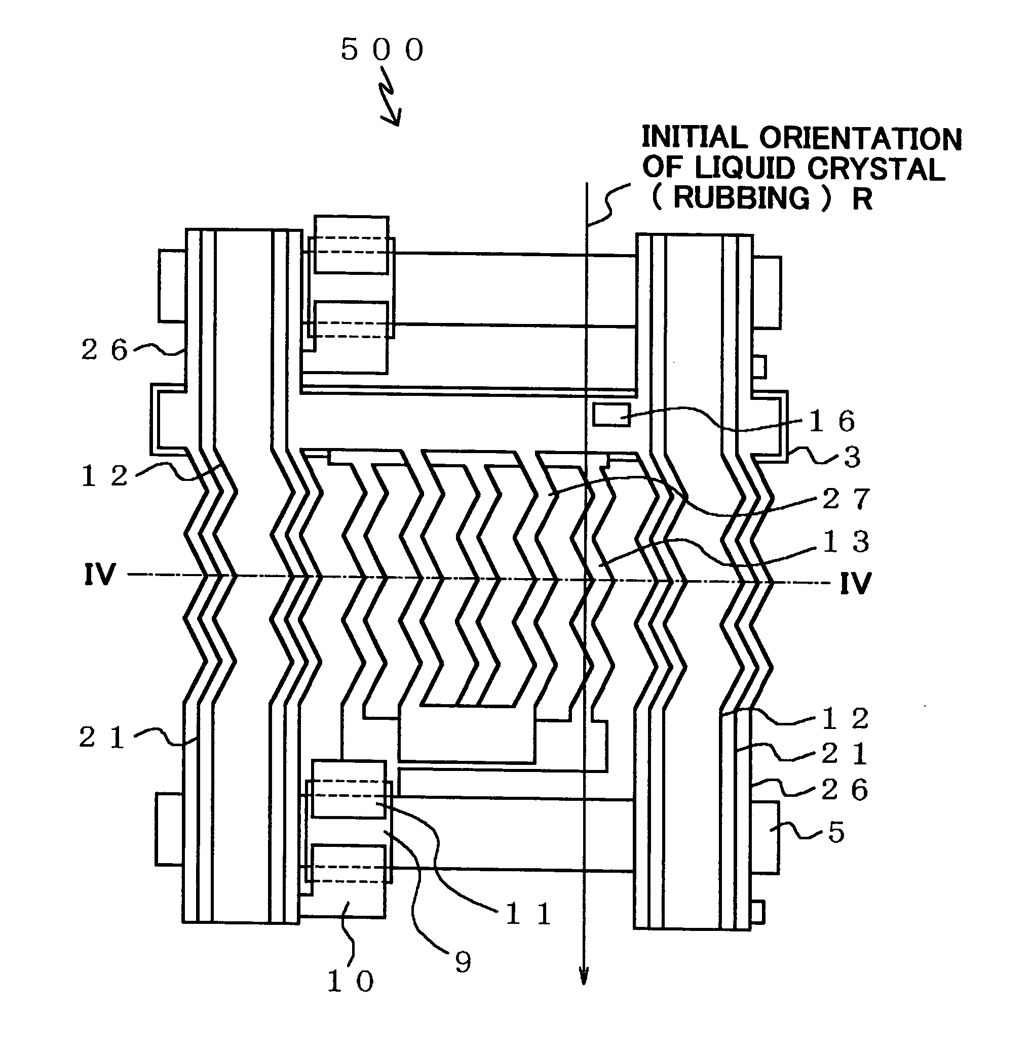
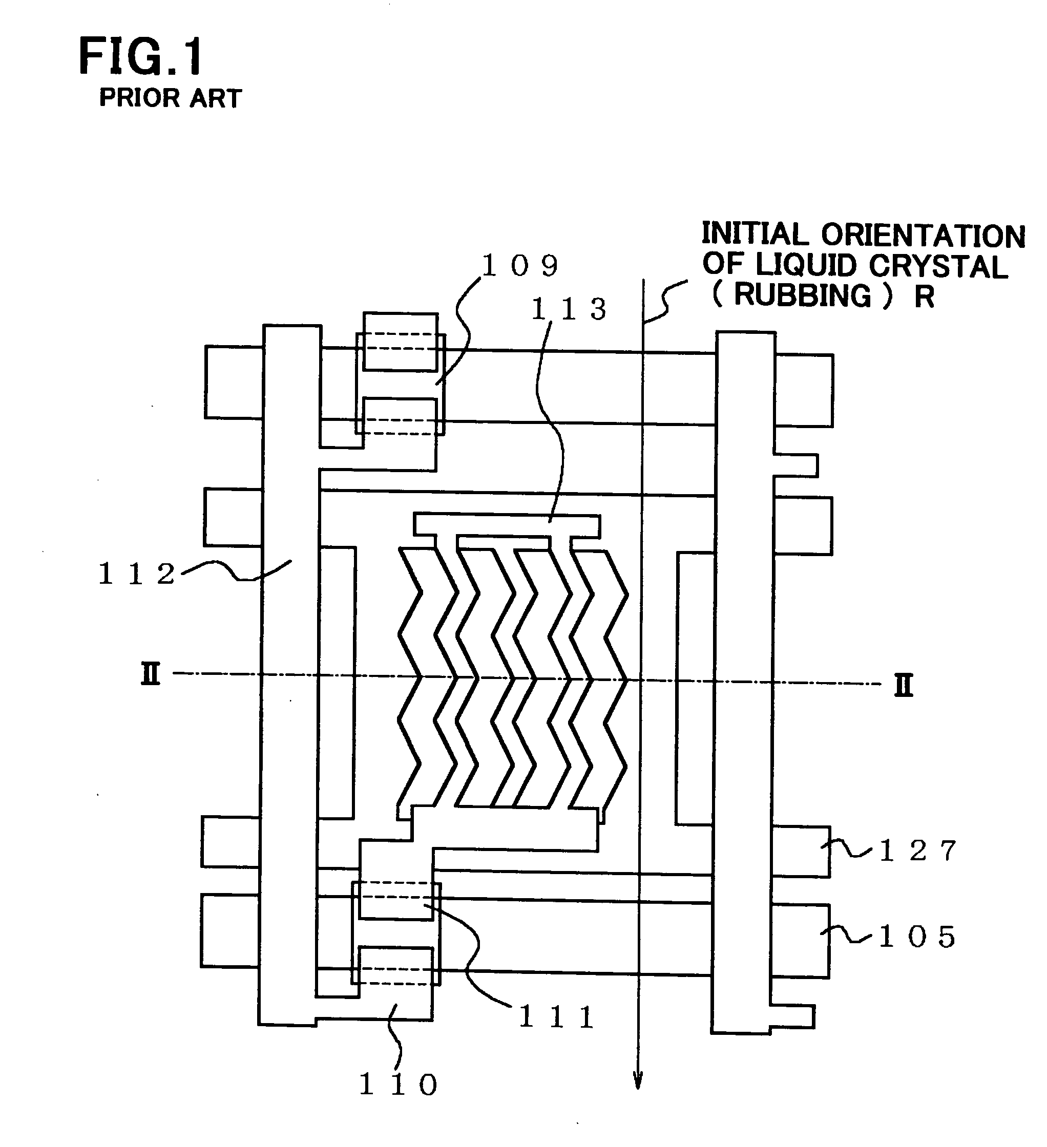
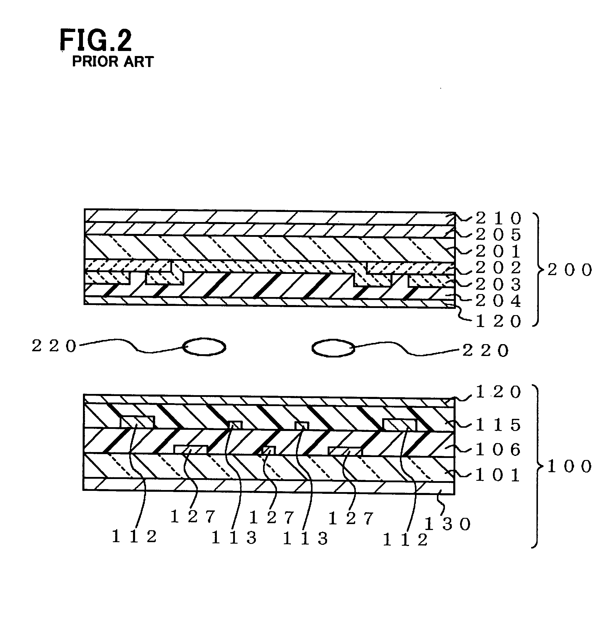
[0262] FIG. 28 is a cross-sectional view of a third example of a TFT substrate in an in-plane switching active matrix type liquid crystal display device which is capable of preventing corrosion of metal which is corroded in atmosphere.
[0263] In the TFT substrate in accordance with the second example, above the data line 12 is formed a first island-shaped electrically insulating organic film 21 composed of novolak resin, which is shielded by the data line shield (electrically conductive transparent film) 26 constituting a common electrode.
[0264] A comb-shaped electrode of the pixel electrode 13 is formed in the same layer as the data line 12, and hence, is composed of the same metal as the metal of which the data line 12 is composed. A comb-shaped electrode of the common electrode 27 is comprised of an electrically conductive transparent film of which the data line shield 26 is comprised, on the inorganic passivation film 15.
[0265] The contact holes 17 and 18 reaching the data line t...
fourth example
[0266] FIG. 29 is a cross-sectional view of a fourth example of a TFT substrate in an-in-plane switching active matrix type liquid crystal display device which is capable of preventing corrosion of metal which is corroded in atmosphere.
[0267] In the TFT substrate in accordance with the second example, above the data line 12 is formed a first island-shaped electrically insulating organic film 21 composed of novolak resin, which is shielded by the data line shield (electrically conductive transparent film) 26 constituting a common electrode.
[0268] A comb-shaped electrode in the common electrode 27 and a comb-shaped electrode in the pixel electrode 13 are comprised of an electrically conductive transparent film. The data line shield (electrically conductive transparent film) 26 and the comb-shaped electrode are comprised only of the second electrically conductive transparent film 28 (or 29, 30).
[0269] The contact hole 16 is formed throughout the first interlayer insulating inorganic fi...
fifth example
[0273] FIG. 30 is a cross-sectional view of a fifth example of a TFT substrate in an in-plane switching active matrix type liquid crystal display device which is capable of preventing corrosion of metal which is corroded in atmosphere.
[0274] In the TFT substrate in accordance with the second example, above the data line 12 is formed a first island-shaped electrically insulating organic film 21 composed of novolak resin, which is shielded by the data line shield (electrically conductive transparent film) 26 constituting a common electrode.
[0275] A comb-shaped electrode in the common electrode 27 and a comb-shaped electrode in the pixel electrode 13 are comprised of an electrically conductive transparent film. The data line shield (electrically conductive transparent film) 26 and the comb-shaped electrode are comprised only of the second electrically conductive transparent film 28 (or 29, 30).
[0276] The contact hole 16 formed in association with a common electrode is covered at its in...
PUM
| Property | Measurement | Unit |
|---|---|---|
| thickness | aaaaa | aaaaa |
| resistivity | aaaaa | aaaaa |
| temperature | aaaaa | aaaaa |
Abstract
Description
Claims
Application Information
 - R&D
- Intellectual Property
- Life Sciences
- Materials
- Tech Scout
- Unparalleled Data Quality
- Higher Quality Content
- 60% Fewer Hallucinations
Browse by: Latest US Patents, China's latest patents, Technical Efficacy Thesaurus, Application Domain, Technology Topic, Popular Technical Reports.
© 2025 PatSnap. All rights reserved.Legal|Privacy policy|Modern Slavery Act Transparency Statement|Sitemap|About US| Contact US: help@patsnap.com