
Compound, composition for forming organic film, substrate for manufacturing semiconductor apparatus, method for forming organic film, and patterning process

a composition and organic film technology, applied in the field of compound, can solve the problems of not having the inability to produce semiconductor devices in a good yield, and the inability to achieve a complete etching selectivity between the photoresist film and the production process of the semiconductor device, etc., to achieve excellent gap filling/planarizing characteristics, improve heat resistance, and improve the effect of

Active Publication Date: 2022-04-19
SHIN ETSU CHEM IND CO LTD
View PDF37 Cites 0 Cited by
  • Summary
  • Abstract
  • Description
  • Claims
  • Application Information

AI Technical Summary

Benefits of technology

This patent describes a new compound that can be used to make films that are resistant to corrosion and have good gap filling and planarizing properties. The compound can be cured in an inert gas to prevent byproducts and can be used to make different types of films with various properties like heat resistance and etching durability. It is useful in various resist processes and can help produce semiconductor devices. The film formed from this compound is heat resistant and stable even when a hard mask is applied to it. Overall, this patent provides a new tool for making high-quality films in semiconductor manufacturing.

Problems solved by technology

Practically, however, there is no dry etching method having a complete etching selectivity between the photoresist film and the substrate to be processed.
On the other hand, the attempt to produce smaller pattern sizes in production processes of semiconductor devices is approaching the inherent limit due to the wavelength of a light source for photolithography.
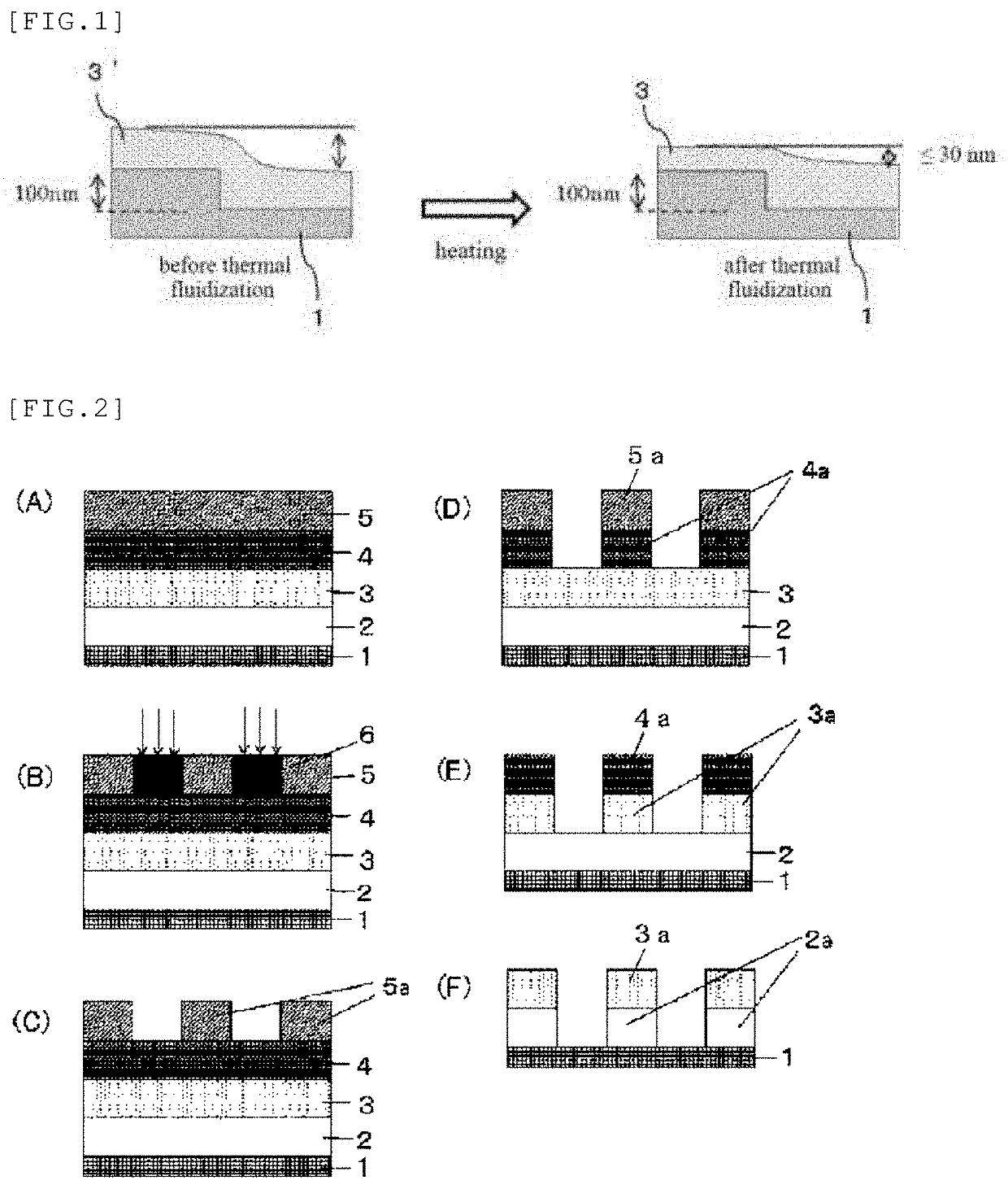
On the other hand, it is difficult to produce semiconductor devices in a good yield by a single layer resist process since it requires an upper layer resist film to have thicker film thickness for gap filling a stepped or patterned substrate to be processed, thereby causing lower tolerance for pattern forming in exposure such as pattern collapse after exposure and development as well as degradation of a pattern profile due to reflection from a substrate in exposure.
This risks the semiconductor device to fail to attain higher processing speed as it is designed, and fail to attain the yield that can be managed as industrial manufacturing.
These material for forming an organic film, however, has insufficient characteristics of gap filling and planarizing a pattern formed on a substrate.

Method used


Image

  • Compound, composition for forming organic film, substrate for manufacturing semiconductor apparatus, method for forming organic film, and patterning process
  • Compound, composition for forming organic film, substrate for manufacturing semiconductor apparatus, method for forming organic film, and patterning process
  • Compound, composition for forming organic film, substrate for manufacturing semiconductor apparatus, method for forming organic film, and patterning process

Examples


synthesis example 1

[Synthesis Example 1] Synthesis of Compound (A1)

[0183]In an N2 atmosphere, to an ice-cooled mixed solution of 12.6 g of 1,3-diethynylbenzen, 36.0 g of 9-fluorenone, and 200 g of toluene, 24.7 g of potassium t-butoxide was added, and this was stirred for 3 hours in an ice bath. The reaction was stopped by adding water, and 200 mL of tetrahydrofuran was added thereto. This was washed with water and concentrated under reduced pressure, and then toluene was added thereto. The formed solid was filtered off, washed with toluene, and dried under reduced pressure to give 42.3 g of Compound (A1).

[0184]

[0185]Shown in the following are analytical results of IR and 1H NMR for the synthesized Compound (A1).

[0186]IR (D-ATR): ν=3310 (br), 3069, 3046, 3023, 1592, 1477, 1450, 1047, 1001, 791, 747, 726 cm−1

[0187]1H NMR (600 MHz, DMSO-d6): δ=7.78 (d, J=7.4 Hz, 4H), 7.70 (d, J=7.4 Hz, 4H), 7.43-7.40 (m, 4H), 7.37-7.34 (m, 7H), 7.32-7.29 (m, 1H), 6.70 (s, 2H) ppm.

synthesis example 2

[Synthesis Example 2] Synthesis of Compound (A2)

[0188]After mixing 9.7 g of Compound (A1), 0.5 g of N,N-dimethyl-4-aminopyridine, and 30 g of pyridine, the mixture was heated to 70° C. To the reaction mixture, 6.1 g of acetic anhydride was added, and this was heated to 80° C. and stirred for 4 hours. After cooling, the reaction was stopped by adding water. To this mixture, 100 mL of toluene and 100 mL of tetrahydrofuran were added. This was washed with water and concentrated under reduced pressure, and then hexane was added thereto. The formed solid was filtered off, washed with hexane, and dried under reduced pressure to give 9.4 g of Compound (A2).

[0189]

[0190]Shown in the following are analytical results of IR and 1H NMR for the synthesized Compound (A2).

[0191]IR (D-ATR): ν=3065, 1745, 1592, 1476, 1450, 1231, 1209, 1050, 1008, 969, 794, 769, 755, 733 cm−1

[0192]1H NMR (600 MHz, DMSO-d6): δ=7.84 (d, J=7.6 Hz, 4H), 7.81 (d, J=7.6 Hz, 4H), 7.49-7.46 (m, 4H), 7.41-7.37 (m, 7H), 7.35-7...

synthesis example 3

[Synthesis Example 3] Synthesis of Compound (A3)

[0193]In an N2 atmosphere, to an ice-cooled mixed solution of 6.3 g of 1,3-diethynylbenzen and 100 g of tetrahydrofuran, 100 mL of 1 N magnesium ethyl bromide solution in tetrahydrofuran was added, and this was slowly warmed to room temperature. To this mixture, 20.2 g of thioxanthone was added, and this was heated to 40° C. and stirred for 24 hours. After cooling, the reaction was stopped by adding water. To this mixture, 200 mL of methyl isobutyl ketone was added. This was washed with water and concentrated under reduced pressure, and then hexane was added thereto. The formed solid was filtered off, washed with hexane, and dried under reduced pressure to give 17.1 g of the intended material (A3).

[0194]

[0195]Shown in the following are analytical results of IR and 1H NMR for the synthesized Compound (A3).

[0196]IR (D-ATR): ν=3299 (br), 3062, 3027, 1581, 1457, 1443, 1354, 1185, 1055, 992, 789, 755, 748, 736 cm−1

[0197]1H NMR (600 MHz, DM...


PUM

PropertyMeasurementUnit
temperatureaaaaaaaaaa

Abstract

A compound including two or more partial structures shown by the following general formula (1-1) in the molecule,wherein each Ar independently represents an aromatic ring optionally having a substituent or an aromatic ring that contains at least one nitrogen atom optionally having a substituent, and two Ars are optionally bonded with each other to form a ring structure; the broken line represents a bond with an organic group; B represents an anionic leaving group that is capable of forming a reactive cation due to effect of either or both of heat and acid. This provides a compound that is capable of curing under the film forming conditions in air or an inert gas without forming byproducts, and forming an organic under layer film that has good dry etching durability during substrate processing not only excellent characteristics of gap filling and planarizing a pattern formed on a substrate.

Description

TECHNICAL FIELD[0001]The present invention relates to a compound, a composition for forming an organic film used in a process for producing a semiconductor device and so on, as well as a substrate for manufacturing a semiconductor apparatus, a method for forming an organic film, and a patterning process using the composition.BACKGROUND ART[0002]Semiconductor devices have been highly integrated and advanced in processing speed by shifting the wavelength of a light source shorter to attain a finer pattern size in lithography technologies using a light exposure (photolithography) as common arts. In order to form such a fine circuit pattern on a semiconductor device substrate (a substrate to be processed), the substrate is usually processed by dry etching using a photoresist film having a formed pattern as an etching mask. Practically, however, there is no dry etching method having a complete etching selectivity between the photoresist film and the substrate to be processed. Accordingly...

Claims


Application Information

Patent Timeline
Patent Type & Authority Patents(United States)
IPC IPC(8): G03F7/025G03F7/11G03F7/09C07D335/12H01L21/027H01L21/311C08F38/00C07C15/56C07C41/01C07C215/46
CPCG03F7/025C07C15/56C07D335/12C08F38/00G03F7/091G03F7/094G03F7/11H01L21/0271H01L21/31138C07C41/01C07C215/46C07C35/38C07C69/16C07D335/16C07C43/2055G03F7/004G03F7/115C07C2603/18G03F7/0037G03F7/027C09D11/101B33Y70/00C07D209/82C07D311/80C07D335/10H01L21/02216H01L21/02288H01L21/324H01L21/31144H01L21/0228G03F7/0002G03F7/075G03F7/095
Inventor TACHIBANA, SEIICHIROWATANABE, TAKERUNIIDA, KEISUKENAGAI, HIROKOSAWAMURA, TAKASHIOGIHARA, TSUTOMU
Owner SHIN ETSU CHEM IND CO LTD
Learn More