
Multilayer printed wiring board production method, adhesive layer-equipped metal foil, metal-clad laminate, and multilayer printed wiring board

a multi-layer printed, wiring board technology, applied in the direction of photosensitive material processing, photomechanical equipment, instruments, etc., can solve the problem of difficult bore, achieve good adhesiveness, enhance the production efficiency of multi-layer printed wiring board having a fine outer layer circui

Active Publication Date: 2021-01-12
RESONAC CORPORATION
View PDF14 Cites 0 Cited by
  • Summary
  • Abstract
  • Description
  • Claims
  • Application Information

AI Technical Summary

Benefits of technology

[0021]In accordance with the present invention, it is possible to provide a production method of a multi-layered printed wiring board capable of not only facilitating the formation of a via hole with a laser at the time of production of a multi-layered wiring board but also forming a fine outer layer circuit, whereby a production efficiency of a multi-layered printed wiring board having a fine outer layer circuit can be remarkably enhanced. Furthermore, it is possible to provide a metal foil with adhesive layer capable of being suitably used for this production method of a multi-layered printed wiring board, which is free from generation of an undercut on laser processing while securing good adhesiveness to plated copper, a metal-clad laminated sheet using the same, and a multi-layered printed wiring board.

Problems solved by technology

But, in the case of forming a via hole on a laminated sheet having a thick copper foil as an outer layer, the copper surface reflects a laser beam, and therefore, boring is difficult.

Method used


Image

  • Multilayer printed wiring board production method, adhesive layer-equipped metal foil, metal-clad laminate, and multilayer printed wiring board
  • Multilayer printed wiring board production method, adhesive layer-equipped metal foil, metal-clad laminate, and multilayer printed wiring board

Examples


production example 1

[0124]Respective components as described below were mixed to obtain a varnish of a resin composition A for adhesive layer (solid concentration: about 70% by mass).

[Thermosetting Resin]

[0125]Novolak type epoxy resin having a biphenyl structure: NC-3000-H (trade name, manufactured by Nippon Kayaku Co., Ltd.): 100 parts by mass

[Polymer Component]

[0126]Carboxylic acid-modified acrylonitrile butadiene rubber particle: XER-91SE-15 (trade name, manufactured by JSR Corporation): 10 parts by mass

[Epoxy Resin Curing Agent]

[0127]Triazine ring-containing cresol novolak type phenol resin: PHENOLITE (registered trademark) LA-3018-50 (trade name, nitrogen content: 18% by mass, hydroxyl group equivalent: 151 g / mol, manufactured by DIC Corporation): 70 parts by mass

[Curing Accelerator]

[0128]Imidazole derivative compound (1-cyanoethyl-2-phenyl imidazolium trimellitate): 2PZ-CNS (trade name, manufactured by Shikoku Chemicals Corporation): 1 part by mass

[Solvent]

[0129]Methyl ethyl ketone

[Production of ...

example 1

[0130]On the surface of an ultrathin copper foil having a copper foil as a support (copper foil thickness of support: 18 μm, thickness of ultrathin copper foil: 3 μm, manufactured by Mitsui Mining & Smelting Co., Ltd., trade name: MT18Ex-3, surface roughness of roughened surface Rz=2.0 μm), the varnish of the composition A for adhesive layer obtained in Production Method 1 was applied and dried at 170° C. for about 10 minutes, thereby obtaining an ultrathin copper foil with adhesive layer. A thickness of the formed organic adhesive layer was 3.0 μm.

[0131]Subsequently, on both surfaces of a substrate with inner layer circuit, on both surfaces of which a blackening-treated inner layer circuit had been formed (material quality: copper, thickness of circuit: 18 μm (on the both surfaces)) (manufactured by Hitachi Chemical Co., Ltd., trade name: MCL-679FG, thickness: 0.5 mm), the above-obtained ultrathin copper foil with adhesive layer was superimposed such that the organic adhesive layer...

production example 2

[0147]Respective components as described below were mixed using a dispersing machine (manufactured by Yoshida Kikai Co., Ltd., trade name: NANOMIZER (registered trademark)) to obtain a varnish of a resin composition B for adhesive layer (solid concentration: about 35% by mass).

[Thermosetting Resin]

[0148]Novolak type epoxy resin having a biphenyl structure: NC-3000S-H (trade name, manufactured by Nippon Kayaku Co., Ltd.): 100 parts by mass

[Polymer Component]

[0149]Carboxylic acid-modified acrylonitrile butadiene rubber particle: XER-91SE-15 (trade name, manufactured by JSR Corporation): 10 parts by mass

[Epoxy Resin Curing Agent]

[0150]Triazine ring-containing cresol novolak type phenol resin: PHENOLITE (registered trademark) LA-3018-50 (trade name, nitrogen content: 18% by mass, hydroxyl group equivalent: 151 g / mol, manufactured by DIC Corporation): 70 parts by mass

[Curing Accelerator]

[0151]1,8-Diazabicycloundecene (DBU) (manufactured by Kanto Chemical Co., Inc.): 1 part by mass

[Inorga...


PUM

PropertyMeasurementUnit
thicknessaaaaaaaaaa
thicknessaaaaaaaaaa
thicknessaaaaaaaaaa

Abstract

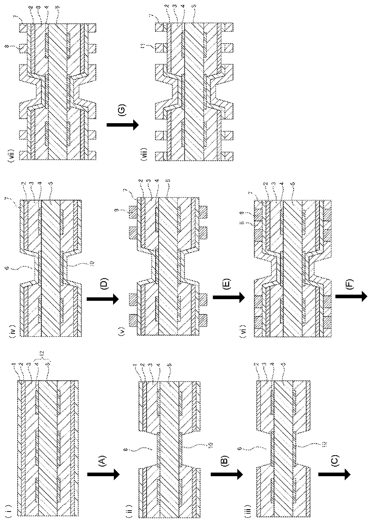
Disclosed is a production method of a multi-layered printed wiring board, including the following steps 1 to 3:Step 1: a step of laminating, on a substrate with inner layer circuit, a metal foil with adhesive layer including a support, a metal foil having a thickness of 3 μm or less and ⅙ or less relative to the thickness of the inner layer circuit, and an organic adhesive layer having a thickness of 10 μm or less in this order, via an organic insulating resin layer such that the organic insulating resin layer and the organic adhesive layer are opposed to each other, and then releasing the support to form a laminated sheet (a) having the metal foil as an outer layer metal foil layer;Step 2: a step of irradiating the laminated sheet (a) with a laser to bore the outer layer metal foil layer, the organic adhesive layer, and the organic insulating resin layer to form a bored laminated sheet (b) having a blind via hole; andStep 3: a step of forming an outer layer circuit connected with the inner layer circuit through the following steps 3-1 to 3-4:Step 3-1: a step of etching removing the outer layer metal foil layer of the bored laminated sheet (b) formed in the step 2 and then forming an outer layer copper layer having a thickness of 2 μm or less on the bored laminated sheet (b);Step 3-2: a step of forming a resist pattern by a resist applied on the outer layer copper layer;Step 3-3: a step of forming a circuit layer on the surface of the outer layer copper layer on which the resist pattern is not formed, by electrolytic copper plating; andStep 3-4: a step of removing the resist pattern and then removing the exposed outer layer copper layer by etching, thereby forming an outer layer circuit connected with the inner layer circuit.

Description

CROSS-REFERENCE TO RELATED APPLICATIONS[0001]This application is a U.S. national phase application filed under 35 U.S.C. § 371 of International Application No. PCT / JP2016 / 073513, filed Aug. 10, 2016, designating the United States, which claims benefit from Japanese Patent Application 2015-158992, filed Aug. 11, 2015, and Japanese Patent Application 2015-158994, filed Aug. 11, 2015, which are hereby incorporated herein by reference in their entirety.TECHNICAL FIELD[0002]The present invention relates a production method of a multi-layered printed wiring board, a metal foil with adhesive layer, a metal-clad laminated sheet, and a multi-layered printed wiring board.BACKGROUND ART[0003]In recent years, following miniaturization, weight reduction, and multi-functionalization of electronic devices, multi-layered printed wiring boards are required to achieve fine wiring and small-diameter of a via hole. It is difficult to perform boring in a diameter of 200 μm or less by means of mechanical...

Claims


Application Information

Patent Timeline
Patent Type & Authority Patents(United States)
IPC IPC(8): H05K3/38G03F7/20H05K3/46H05K3/00C09J163/00G03F7/26H05K3/06H05K3/18H05K3/42G03F7/038H05K1/11
CPCH05K3/386C09J163/00G03F7/2002G03F7/26H05K3/007H05K3/0035H05K3/061H05K3/188H05K3/4644H05K3/4652H05K3/4682G03F7/038H05K1/115H05K3/429H05K3/4673H05K2203/0562H05K2203/0723H05K1/09
Inventor ONOZEKI, HITOSHIINOUE, TSUBASAYAMAGISHI, KATSUJISHIMIZU, HIROSHI
Owner RESONAC CORPORATION
Learn More